ZHCSCY3E October 2014 – October 2018 LM5160 , LM5160A
PRODUCTION DATA.
- 1 特性
- 2 应用
- 3 说明
- 4 修订历史记录
- 5 Pin Configuration and Functions
- 6 Specifications
- 7 Detailed Description
-
8 Application and Implementation
- 8.1 Application Information
- 8.2
Typical Applications
- 8.2.1
LM5160 Synchronous Buck (10-V to 60-V Input, 5-V Output, 1.5-A Load)
- 8.2.1.1 Design Requirements
- 8.2.1.2
Detailed Design Procedure
- 8.2.1.2.1 Custom Design With WEBENCH® Tools
- 8.2.1.2.2 Feedback Resistor Divider - RFB1, RFB2
- 8.2.1.2.3 Switching Frequency - RON
- 8.2.1.2.4 Inductor - L
- 8.2.1.2.5 Output Capacitor - COUT
- 8.2.1.2.6 Series Ripple Resistor - RESR
- 8.2.1.2.7 VCC and Bootstrap Capacitors - CVCC, CBST
- 8.2.1.2.8 Input Capacitor - CIN
- 8.2.1.2.9 Soft-Start Capacitor - CSS
- 8.2.1.2.10 EN/UVLO Resistors - RUV1, RUV2
- 8.2.1.3 Application Curves
- 8.2.2 LM5160 Isolated Fly-Buck (18-V to 32-V Input, 12-V, 4.5-W Isolated Output)
- 8.2.3 LM5160A Isolated Fly-Buck (18-V to 32-V Input, 12-V, 4.5-W Isolated Output)
- 8.2.1
LM5160 Synchronous Buck (10-V to 60-V Input, 5-V Output, 1.5-A Load)
- 8.3 Do's and Don'ts
- 9 Power Supply Recommendations
- 10Layout
- 11器件和文档支持
- 12机械、封装和可订购信息
8.2.3 LM5160A Isolated Fly-Buck (18-V to 32-V Input, 12-V, 4.5-W Isolated Output)
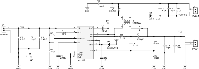
The LM5160A when used in either the buck or the Fly-Buck application, can also be biased by an external voltage source for improved efficiency requirements. The LM5160A can be externally biased to VOUT by connecting VCC to VOUT through a diode as shown in the Fly-Buck application circuit in Figure 35. In this dual output rail Fly-Buck application circuit, the VCC pin is externally diode connected (D2) to VOUT (primary). The design procedure with the LM5160A, for both Buck and Fly-Buck configurations, remains the same as with LM5160. The voltage applied to the VCC pin, either from VOUT or an external supply must be between 9 V and 13 V.
 Figure 35. LM5160A 12-V, 4.5-W Fly-Buck Isolated Converter Schematic