ZHCSGB0B November 2017 – November 2020 LM5145
PRODUCTION DATA
- 1 特性
- 2 应用
- 3 说明
- 4 Revision History
- 5 Description (continued)
- 6 Pin Configuration and Functions
- 7 Specifications
-
8 Detailed Description
- 8.1 Overview
- 8.2 Functional Block Diagram
- 8.3
Feature Description
- 8.3.1 Input Range (VIN)
- 8.3.2 Output Voltage Setpoint and Accuracy (FB)
- 8.3.3 High-Voltage Bias Supply Regulator (VCC)
- 8.3.4 Precision Enable (EN/UVLO)
- 8.3.5 Power Good Monitor (PGOOD)
- 8.3.6 Switching Frequency (RT, SYNCIN)
- 8.3.7 Configurable Soft Start (SS/TRK)
- 8.3.8 Voltage-Mode Control (COMP)
- 8.3.9 Gate Drivers (LO, HO)
- 8.3.10 Current Sensing and Overcurrent Protection (ILIM)
- 8.3.11 OCP Duty Cycle Limiter
- 8.4 Device Functional Modes
-
9 Application and Implementation
- 9.1 Application Information
- 9.2
Typical Applications
- 9.2.1 Design 1 – 20-A High-Efficiency Synchronous Buck Regulator for Telecom Power Applications
- 9.2.2 Design 2 – High Density, 12-V, 10-A Rail With LDO Low-Noise Auxiliary Output for RF Power Applications
- 9.2.3 Design 3 – 150-W, Regulated 24-V Rail for Commercial Drone Applications With Output Voltage Tracking Feature
- 9.2.4 Design 4 – Powering a Multicore DSP From a 24-V or 48-V Rail
- 10Power Supply Recommendations
- 11Layout
- 12Device and Documentation Support
- 13Mechanical, Packaging, and Orderable Information
9.1.2.3 Input Capacitors
Input capacitors are necessary to limit the input ripple voltage to the buck power stage due to switching-frequency AC currents. TI recommends using X5R or X7R dielectric ceramic capacitors to provide low impedance and high RMS current rating over a wide temperature range. To minimize the parasitic inductance in the switching loop, position the input capacitors as close as possible to the drain of the high-side MOSFET and the source of the low-side MOSFET. The input capacitor RMS current is given by Equation 11.
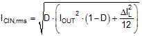
The highest input capacitor RMS current occurs at D = 0.5, at which point the RMS current rating of the capacitors should be greater than half the output current.
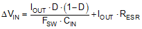
Ideally, the DC component of input current is provided by the input voltage source and the AC component by the input filter capacitors. Neglecting inductor ripple current, the input capacitors source current of amplitude (IOUT − IIN) during the D interval and sinks IIN during the 1−D interval. Thus, the input capacitors conduct a square-wave current of peak-to-peak amplitude equal to the output current. It follows that the resultant capacitive component of AC ripple voltage is a triangular waveform. Together with the ESR-related ripple component, the peak-to-peak ripple voltage amplitude is given by Equation 12.
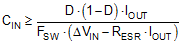
The input capacitance required for a particular load current, based on an input voltage ripple specification of ΔVIN, is given by Equation 13.
Low-ESR ceramic capacitors can be placed in parallel with higher valued bulk capacitance to provide optimized input filtering for the regulator and damping to mitigate the effects of input parasitic inductance resonating with high-Q ceramics. One bulk capacitor of sufficiently high current rating and two or three 2.2-μF 100-V X7R ceramic decoupling capacitors are usually sufficient. Select the input bulk capacitor based on its ripple current rating and operating temperature.