ZHCSGB0B November 2017 – November 2020 LM5145
PRODUCTION DATA
- 1 特性
- 2 应用
- 3 说明
- 4 Revision History
- 5 Description (continued)
- 6 Pin Configuration and Functions
- 7 Specifications
-
8 Detailed Description
- 8.1 Overview
- 8.2 Functional Block Diagram
- 8.3
Feature Description
- 8.3.1 Input Range (VIN)
- 8.3.2 Output Voltage Setpoint and Accuracy (FB)
- 8.3.3 High-Voltage Bias Supply Regulator (VCC)
- 8.3.4 Precision Enable (EN/UVLO)
- 8.3.5 Power Good Monitor (PGOOD)
- 8.3.6 Switching Frequency (RT, SYNCIN)
- 8.3.7 Configurable Soft Start (SS/TRK)
- 8.3.8 Voltage-Mode Control (COMP)
- 8.3.9 Gate Drivers (LO, HO)
- 8.3.10 Current Sensing and Overcurrent Protection (ILIM)
- 8.3.11 OCP Duty Cycle Limiter
- 8.4 Device Functional Modes
-
9 Application and Implementation
- 9.1 Application Information
- 9.2
Typical Applications
- 9.2.1 Design 1 – 20-A High-Efficiency Synchronous Buck Regulator for Telecom Power Applications
- 9.2.2 Design 2 – High Density, 12-V, 10-A Rail With LDO Low-Noise Auxiliary Output for RF Power Applications
- 9.2.3 Design 3 – 150-W, Regulated 24-V Rail for Commercial Drone Applications With Output Voltage Tracking Feature
- 9.2.4 Design 4 – Powering a Multicore DSP From a 24-V or 48-V Rail
- 10Power Supply Recommendations
- 11Layout
- 12Device and Documentation Support
- 13Mechanical, Packaging, and Orderable Information
9.1.4 EMI Filter Design
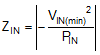
Switching regulators exhibit negative input impedance, which is lowest at the minimum input voltage. An underdamped LC filter exhibits a high output impedance at the resonant frequency of the filter. For stability, the filter output impedance must be less than the absolute value of the converter input impedance.
The EMI filter design steps are as follows:
- Calculate the required attenuation of the EMI filter at the switching frequency, where CIN represents the existing capacitance at the input of the switching converter.
- Input filter inductor LIN is usually selected between 1 μH and 10 μH, but it can be lower to reduce losses in a high current design.
- Calculate input filter capacitor CF full stop.
 Figure 9-4 Buck Regulator With π-Stage EMI Filter
By calculating the first harmonic current from the Fourier series of the input current waveform and multiplying it by the input impedance (the impedance is defined by the existing input capacitor CIN), a formula is derived to obtain the required attenuation as shown by Equation 18.
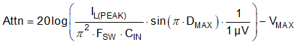
where
- VMAX is the noise specification in dBμV from the applicable EMI standard, for example CISPR 32 Class B.
- CIN is the existing input capacitance of the buck regulator.
- DMAX is the maximum duty cycle.
- IPEAK is the peak inductor current.
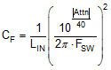
For filter design purposes, the current at the input can be modeled as a square-wave. Determine the EMI filter capacitance CF from Equation 19.
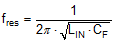
Adding an input filter to a switching regulator modifies the control-to-output transfer function. The output impedance of the filter must be sufficiently small such that the input filter does not significantly affect the loop gain of the buck converter. The impedance peaks at the filter resonant frequency. The resonant frequency of the filter is given by Equation 20.
The purpose of RD is to reduce the peak output impedance of the filter at the resonant frequency. Capacitor CD blocks the DC component of the input voltage to avoid excessive power dissipation in RD. Capacitor CD must have lower impedance than RD at the resonant frequency with a capacitance value greater than that of the input capacitor CIN. This prevents CIN from interfering with the cutoff frequency of the main filter. Added damping is needed when the output impedance of the filter is high at the resonant frequency (Q of filter formed by LIN and CIN is too high). An electrolytic capacitor CD can be used for damping with a value given by Equation 21.

Select the damping resistor RD using Equation 22.
