ZHCSFB5D July 2016 – December 2017 LM5141-Q1
PRODUCTION DATA.
- 1 特性
- 2 应用
- 3 说明
- 4 修订历史记录
- 5 Pin Configuration and Functions
- 6 Specifications
-
7 Detailed Description
- 7.1 Overview
- 7.2 Functional Block Diagram
- 7.3
Feature Description
- 7.3.1 High Voltage Start-up Regulator
- 7.3.2 VCC Regulator
- 7.3.3 Oscillator
- 7.3.4 Synchronization
- 7.3.5 Frequency Dithering (Spread Spectrum)
- 7.3.6 Enable
- 7.3.7 Power Good
- 7.3.8 Output Voltage
- 7.3.9 Current Sense
- 7.3.10 DCR Current Sensing
- 7.3.11 Error Amplifier and PWM Comparator
- 7.3.12 Slope Compensation
- 7.3.13 Hiccup Mode Current Limiting
- 7.3.14 Standby Mode
- 7.3.15 Soft Start
- 7.3.16 Diode Emulation
- 7.3.17 High- and Low-Side Drivers
-
8 Application and Implementation
- 8.1 Application Information
- 8.2 Typical Application
- 9 Power Supply Recommendations
- 10Layout
- 11器件和文档支持
- 12机械、封装和可订购信息
7.3.9 Current Sense
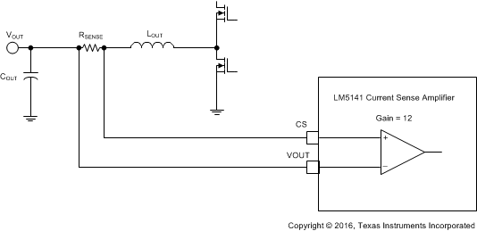
There are two methods to sense the inductor current of the buck converter. The first is using current sense resistor in series with the inductor and the second is to use the dc resistance of the inductor (DCR sensing). Figure 24 shows inductor current sensing using a current-sense resistor. This configuration continuously monitors the inductor current providing accurate current-limit protection. For the best current-sense accuracy and overcurrent protection, use a low inductance ±1% tolerance current-sense resistor between the inductor and output, with a Kelvin connection to the LM5141-Q1 sense amplifier.
If the peak differential current signal sensed from CS to VOUT exceeds 75 mV, the current limit comparator immediately terminates the HO output for cycle-by-cycle current limiting.

where
- V(CS) = 75 mV
IOUT(MAX) is the overcurrent setpoint, which is set higher than the maximum load current to avoid tripping the over current comparator during load transients. ΔI is the peak-peak inductor ripple current.
 Figure 24. Current Sense