ZHCSI53A May 2018 – November 2018 LM5122ZA
PRODUCTION DATA.
- 1 特性
- 2 应用
- 3 说明
- 4 修订历史记录
- 5 Pin Configuration and Functions
- 6 Specifications
-
7 Detailed Description
- 7.1 Overview
- 7.2 Functional Block Diagram
- 7.3
Feature Description
- 7.3.1 Undervoltage Lockout (UVLO)
- 7.3.2 High-Voltage VCC Regulator
- 7.3.3 Oscillator
- 7.3.4 Slope Compensation
- 7.3.5 Error Amplifier
- 7.3.6 PWM Comparator
- 7.3.7 Soft Start
- 7.3.8 HO and LO Drivers
- 7.3.9 Bypass Operation (VOUT = VIN)
- 7.3.10 Cycle-by-Cycle Current Limit
- 7.3.11 Clock Synchronization
- 7.3.12 Maximum Duty Cycle
- 7.3.13 Thermal Protection
- 7.4 Device Functional Modes
-
8 Application and Implementation
- 8.1
Application Information
- 8.1.1 Feedback Compensation
- 8.1.2 Sub-Harmonic Oscillation
- 8.1.3 Interleaved Boost Configuration
- 8.1.4 DCR Sensing
- 8.1.5 Output Overvoltage Protection
- 8.1.6 SEPIC Converter Simplified Schematic
- 8.1.7 Non-Isolated Synchronous Flyback Converter Simplified Schematic
- 8.1.8 Negative to Positive Conversion
- 8.2
Typical Application
- 8.2.1 Design Requirements
- 8.2.2
Detailed Design Procedure
- 8.2.2.1 Timing Resistor RT
- 8.2.2.2 UVLO Divider RUV2, RUV1
- 8.2.2.3 Input Inductor LIN
- 8.2.2.4 Current Sense Resistor RS
- 8.2.2.5 Current Sense Filter RCSFP, RCSFN, CCS
- 8.2.2.6 Slope Compensation Resistor RSLOPE
- 8.2.2.7 Output Capacitor COUT
- 8.2.2.8 Input Capacitor CIN
- 8.2.2.9 VIN Filter RVIN, CVIN
- 8.2.2.10 Bootstrap Capacitor CBST and Boost Diode DBST
- 8.2.2.11 VCC Capacitor CVCC
- 8.2.2.12 Output Voltage Divider RFB1, RFB2
- 8.2.2.13 Soft-Start Capacitor CSS
- 8.2.2.14 Restart Capacitor CRES
- 8.2.2.15 Low-Side Power Switch QL
- 8.2.2.16 High-Side Power Switch QH and Additional Parallel Schottky Diode
- 8.2.2.17 Snubber Components
- 8.2.2.18 Loop Compensation Components CCOMP, RCOMP, CHF
- 8.2.3 Application Curves
- 8.1
Application Information
- 9 Power Supply Recommendations
- 10Layout
- 11器件和文档支持
- 12机械、封装和可订购信息
7.3.4 Slope Compensation
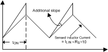
For duty cycles greater than 50%, peak-current-mode regulators are subject to sub-harmonic oscillation. Sub-harmonic oscillation is normally characterized by observing alternating wide and narrow duty cycles. This sub-harmonic oscillation can be eliminated by a technique, which adds an artificial ramp, known as slope compensation, to the sensed inductor current.
 Figure 20. Slope Compensation
 The amount of slope compensation is programmable by a single resistor connected between the SLOPE pin and the AGND pin. The amount of slope compensation can be calculated as follows:

where
RSLOPE value can be determined from Equation 6 at minimum input voltage:

where
- K = 0.82~1 as a default
From Equation 6, K can be calculated over the input range as follows:

where
In any case, K should be greater than at least 0.5. At higher switching frequency over 500 kHz, TI recommends that K factor be greater than or equal to 1 because the minimum on-time affects the amount of slope compensation due to internal delays.
The sum of sensed inductor current and slope compensation should be less than COMP output high voltage (VOH) for proper startup with load and proper current limit operation. This limits the minimum value of RSLOPE to be:

where
- This equation can be used in most cases
- Consider this conservative selection when VIN(MIN) < 5.5 V

where
The SLOPE pin cannot be left floating.

