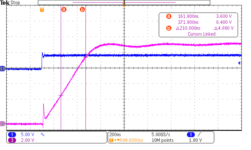
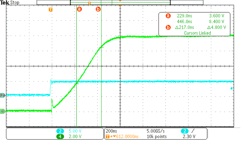
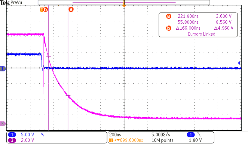
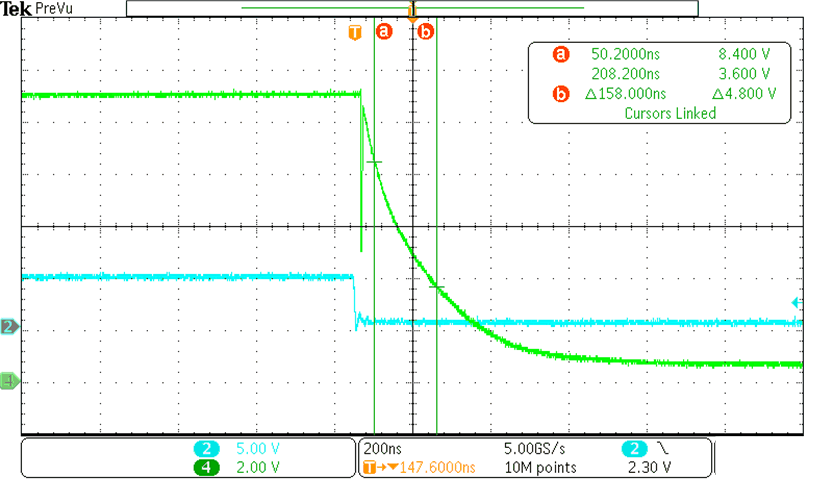
To minimize the switching losses in power supplies, turn-ON and turn-OFF of the power MOSFETs need to be as fast as possible. Higher the drive current capability of the driver, faster the switching. Therefore, the LM5108 is designed with high drive current capability and low resistance of the output stages. One of the common way to test the drive capability of the gate driver device , is to test it under heavy load. Rise time and fall time of the outputs would provide idea of drive capability of the gate driver device. There must not be any resistance in this test circuit. Figure 8-2 and Figure 8-3 shows rise time and fall time of HO respectively of LM5108. Figure 8-4 and Figure 8-5 shows rise time and fall time of LO respectively of LM5108. For accuracy purpose, the VDD and HB pin of the gate driver device were connected together. HS and VSS pins are also connected together for this test.
Peak current capability can be estimated using the fastest dV/dt along the rise and fall curve of the plot. This method is also useful in comparing performance of two or more gate driver devices.
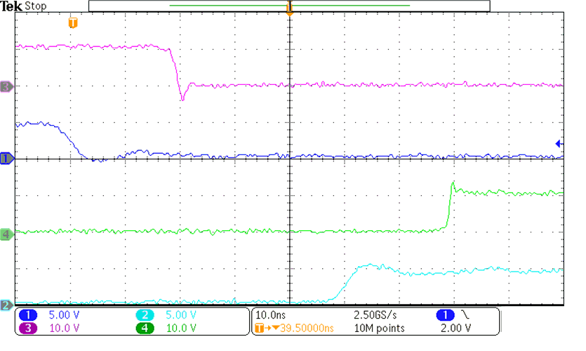
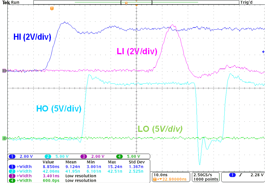
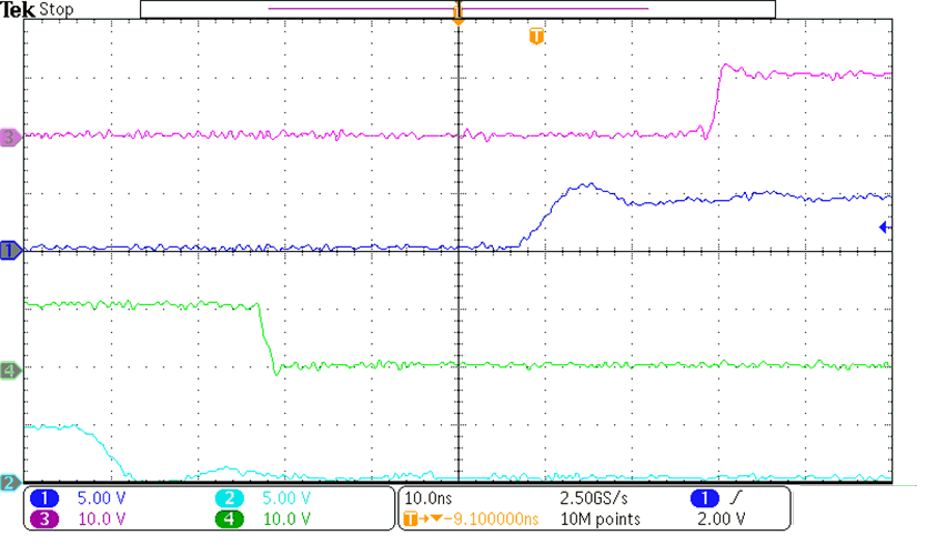
As explained in Section 8.2.2.4, propagation delay plays an important role in reliable operation of many applications. Figure 8-6 and Figure 8-7 shows propagation delays of LM5108. In many switching power supply applications input signals to the gate driver have large amplitude high frequency noise. If there is no filter employed at the input, then there is a possibility of false signal passing through the gate driver and causing shoot-through on the output. LM5108 prevents such shoot-through. If two inputs are high at the same time, LM5108 shuts both the outputs off. Figure 8-8 shows interlock feature of LM5108.

| VDD=VHB=12 V, HS=VSS |
CLOAD=68
nF |
Ch1=HI, Ch3=HO |
Figure 8-2 HO
Rise Time
| VDD=VHB=12 V, HS=VSS |
CLOAD=68
nF |
Ch2=LI, Ch4=LO |
Figure 8-4 LO Rise Time
| VDD=VHB=12 V, HS=VSS |
CLOAD=No
load |
Ch1=HI Ch2=LI Ch3=HO
Ch4=LO |
Figure 8-6 Propagation Delay
| VDD=VHB=12 V, HS=VSS |
CLOAD=0
nF |
|
Figure 8-8 Shoot-through Protection or Interlock
| VDD=VHB=12 V, HS=VSS |
CLOAD=68
nF |
Ch1=HI, Ch3=HO |
Figure 8-3 HO
Fall Time
| VDD=VHB=12 V, HS=VSS |
CLOAD=68
nF |
Ch2=LI, Ch4=LO |
Figure 8-5 LO Fall Time
| VDD=VHB=12 V, HS=VSS |
CLOAD=No
load |
Ch1=HI Ch2=LI Ch3=HO
Ch4=LO |
Figure 8-7 Propagation Delay