SNVS215D April 2003 – November 2015 LM5030
PRODUCTION DATA.
- 1 Features
- 2 Applications
- 3 Description
- 4 Revision History
- 5 Pin Configuration and Functions
- 6 Specifications
- 7 Detailed Description
- 8 Application and Implementation
- 9 Power Supply Recommendations
- 10Layout
- 11Device and Documentation Support
- 12Mechanical, Packaging, and Orderable Information
封装选项
机械数据 (封装 | 引脚)
散热焊盘机械数据 (封装 | 引脚)
- DPR|10
订购信息
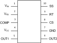
5 Pin Configuration and Functions
DGS, DPR Package
10-Pin VSSOP, WSON
Top View

Pin Functions
| PIN | I/O | DESCRIPTION | APPLICATION INFORMATION | |
|---|---|---|---|---|
| NAME | NO. | |||
| COMP | 3 | O | Output to the error amplifier | There is an internal 5-kΩ pullup resistor on this pin. The error amplifier provides an active sink. |
| CS | 8 | I | Current sense input | Current sense input for current mode control and current limit sensing. Using separate dedicated comparators, if CS exceeds 0.5 V, the outputs will go into cycle-by-cycle current limit. If CS exceeds 0.625 V the outputs will be disabled and a softstart commenced. |
| GND | 7 | — | Return | Ground |
| OUT1 | 5 | O | Output of the PWM controller | Alternating PWM output gate driver |
| OUT2 | 6 | O | Output of the PWM controller | Alternating PWM output gate driver |
| RT | 9 | I | Oscillator timing resistor pin and synchronization input | An external resistor sets the oscillator frequency. This pin will also accept synchronization pulses from an external oscillator. |
| SS | 10 | I | Dual purpose soft start and shutdown pin | A 10-µA current source and an external capacitor set the softstart timing length. The controller will enter a low power state if the SS pin is pulled below the typical shutdown threshold of 0.45 V. |
| VIN | 1 | I | Source input voltage | Input to start-up regulator. Input range 14 to 100 V. |
| VFB | 2 | I | Inverting input to the error amplifier | The non-inverting input is internally connected to a 1.25-V reference. |
| VCC | 4 | I/O | Output from the internal high-voltage series pass regulator. The regulation setpoint is 7.7 V. |
If an auxiliary winding raises the voltage on this pin above the regulation setpoint, the internal series pass regulator will shutdown, reducing the IC power dissipation. |
| WSON DAP |
SUB | — | Die substrate | The exposed die attach pad on the WSON package should be connected to a PCB thermal pad at ground potential. For additional information on using TI's No Pull Back WSON package, refer to WSON Application Note AN-1187 (SNOA401). |