SNVS215D April 2003 – November 2015 LM5030
PRODUCTION DATA.
- 1 Features
- 2 Applications
- 3 Description
- 4 Revision History
- 5 Pin Configuration and Functions
- 6 Specifications
- 7 Detailed Description
- 8 Application and Implementation
- 9 Power Supply Recommendations
- 10Layout
- 11Device and Documentation Support
- 12Mechanical, Packaging, and Orderable Information
封装选项
机械数据 (封装 | 引脚)
散热焊盘机械数据 (封装 | 引脚)
- DPR|10
订购信息
10 Layout
10.1 Layout Guidelines
As in all high frequency switching power supplies, it is important to separate the high current return trace from the low level GND signal of the controller. These signals should be connected together at a single point, usually the negative side of the DC input filter capacitor.
Layout considerations are critical for the current sense filter. If a current sense transformer is used, both leads of the transformer secondary should be routed to the sense filter components and to the device pins. If the current sense circuit employs a sense resistor in the power MOSFET source, a low inductance resistor should be used and all the low current traces should be connected in common near the device with a single connection made to the GND pin.
The gate drive outputs of the device should have short, direct paths to the power MOSFETs in order to minimize inductance in the gate path.
If the internal dissipation of the device produces a high junction temperature during normal operation, the use of multiple vias under the device to a ground plane can help conduct heat away from the device.
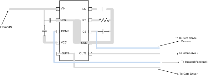
10.2 Layout Example
 Figure 14. LM5030 Board Layout