SNVS961E APRIL 2013 – January 2016 LM5023
PRODUCTION DATA.
- 1 Features
- 2 Applications
- 3 Description
- 4 Revision History
- 5 Pin Configuration and Functions
- 6 Specifications
-
7 Detailed Description
- 7.1 Overview
- 7.2 Functional Block Diagram
- 7.3 Feature Description
- 7.4 Device Functional Modes
- 8 Application and Implementation
- 9 Power Supply Recommendations
- 10Layout
- 11Device and Documentation Support
- 12Mechanical, Packaging, and Orderable Information
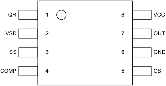
5 Pin Configuration and Functions
Pin Functions
| PIN | TYPE | DESCRIPTION | |
|---|---|---|---|
| NAME | NO. | ||
| COMP | 4 | I | Control input for the pulse width modulator and skip cycle comparators. COMP pullup is provided by an internal 42-kΩ resistor which may be used to bias an opto-coupler transistor. |
| CS | 5 | I | Current sense input for current-mode control and over-current protection. Current limiting is accomplished using a dedicated current sense comparator. If the CS comparator input exceeds 0.5 V, the OUT pin switches low for cycle-by-cycle current limit. CS is held low for 130 ns after OUT switches high to blank the leading edge current spike. |
| GND | 6 | G | Ground connection return for internal circuits. |
| OUT | 7 | O | High current output to the external MOSFET gate input with source/sink current capability of 0.3 A and 0.7 A respectively. |
| QR | 1 | I | The auxiliary flyback winding of the power transformer is monitored to detect the quasi-resonant operation. The peak-auxiliary voltage is sensed to detect an output overvoltage (OVP) fault and shuts down the controller. |
| SS | 3 | O | An external capacitor and an internal 22-µA current source sets the soft-start ramp. |
| VSD | 2 | O | Connect this pin to the gate of the external start-up circuit FET; it disables the start-up FET after VCC is valid. |
| VCC | 8 | P | VCC provides bias to controller and gate drive sections of the LM5023. An external capacitor must be connected from this pin to ground. |
