SNVS961E APRIL 2013 – January 2016 LM5023
PRODUCTION DATA.
- 1 Features
- 2 Applications
- 3 Description
- 4 Revision History
- 5 Pin Configuration and Functions
- 6 Specifications
-
7 Detailed Description
- 7.1 Overview
- 7.2 Functional Block Diagram
- 7.3 Feature Description
- 7.4 Device Functional Modes
- 8 Application and Implementation
- 9 Power Supply Recommendations
- 10Layout
- 11Device and Documentation Support
- 12Mechanical, Packaging, and Orderable Information
8 Application and Implementation
NOTE
Information in the following applications sections is not part of the TI component specification, and TI does not warrant its accuracy or completeness. TI’s customers are responsible for determining suitability of components for their purposes. Customers should validate and test their design implementation to confirm system functionality.
8.1 Application Information
The LM5023 is a quasi-resonant PWM controller optimized for isolated flyback converters with secondary-side regulation. The controller can be used with single or multiple output converters. Applications include notebook adapters and a variety of consumer and industrial applications. The skip-cycle operation, reduced device bias current and control for high-voltage start-up circuit facilitates achieving low-standby input power.
8.2 Typical Application
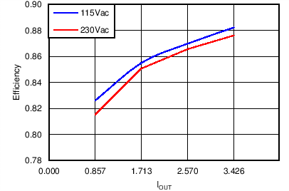
This AC-to-DC adapter, 19.2-V, 65-W design example describes the design of a 65-W off-line flyback converter providing 19.2 V at 3.43-A maximum load and operating from a universal AC input. The design uses the LM5023 AC-to-DC quasi-resonant primary-side controller in a DCM type flyback converter and achieves 88% full load efficiency.
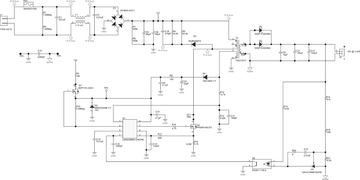 Figure 13. LM5023 Typical Application
8.2.1 Design Requirements
Table 1 lists the design requirements for the LM5023.
Table 1. LM5023 Performance Specifications
| PARAMETER | TEST CONDITION | MIN | TYP | MAX | UNITS | |
|---|---|---|---|---|---|---|
| INPUT CHARACTERISTICS | ||||||
| VIN | Input voltage | 90 | 115/230 | 264 | VAC | |
| VIN | No load input power | VIN = 230 V | 30 | mW | ||
| OUTPUT CHARACTERISTICS | ||||||
| VOUT | Output voltage | VIN = 115 V, IOUT = 3.43 A | 19.0 | 19.2 | 19.4 | V |
| VOUT | Line regulation | VIN = min to max, IOUT = max | 1.0% | |||
| VOUT | Load regulation | VIN = nom, IOUT = no load to max load | 1.0% | |||
| VOUT | Output voltage ripple | VIN = nom, IOUT = max load | 100 | mVPP | ||
| IOUT | Output current | 3.43 | A | |||
| VOVP | Output OVP | 24 | V | |||
| M | Load step response | IOUT = 0.343 A to 3.09 A, 3.09 A to 0.343 A | 18.7 | 19.6 | V | |
| SYSTEMS CHARACTERISTICS | ||||||
| Switching frequency | 130 | kHz | ||||
| η | Full load | VIN = 115/230 V, IOUT = 3.43 A | 88% | |||
8.2.2 Detailed Design Procedure
8.2.2.1 Custom Design with WEBENCH Tools
Click here to create a custom design using the LM5023 device with the WEBENCH® Power Designer.
- Start by entering your VIN, VOUT and IOUT requirements.
- Optimize your design for key parameters like efficiency, footprint and cost using the optimizer dial and compare this design with other possible solutions from Texas Instruments.
- WEBENCH Power Designer provides you with a customized schematic along with a list of materials with real time pricing and component availability.
- In most cases, you will also be able to:
- Run electrical simulations to see important waveforms and circuit performance,
- Run thermal simulations to understand the thermal performance of your board,
- Export your customized schematic and layout into popular CAD formats,
- Print PDF reports for the design, and share your design with colleagues.
- Get more information about WEBENCH tools at www.ti.com/webench.
8.2.2.2 Line Current-Limit Feedforward
In a peak-current mode controlled when the power supply is in an overload, the peak current (measured across the current sense resistor VCS) is compared to a voltage reference for overload protection. If the peak current exceeds the reference the LM5023 controller will turn off the primary-side flyback MOSFET on a cycle-by-cycle basis. However, the primary switch can’t be turned off instantly, as there are several unavoidable delays. The first delay is caused by the LEB circuit which provides leading-edge blanking. The second delay is caused by the propagation delay between the detecting point of VCS and the actual turn off of the power MOSFET. The total delay time (tPROP) refer to Figure 14, includes the current limit comparator, the logic, the gate driver, and the power MOSFET turning off.
The propagation delay causes the peak-primary current to overshoot, the overshoot increase the maximum peak current beyond the calculated value. The peak-current overshoot increase as the AC line voltage increase because of the increase in the slope of the primary current, shown in Equation 20.

This increase in the peak-input-current overshoot causes a wide variation of overpower limit in a flyback converter. In Figure 4, the overpower limit increases with the input line voltage because of IPK(max) increase shown in Equation 21 through Equation 23.


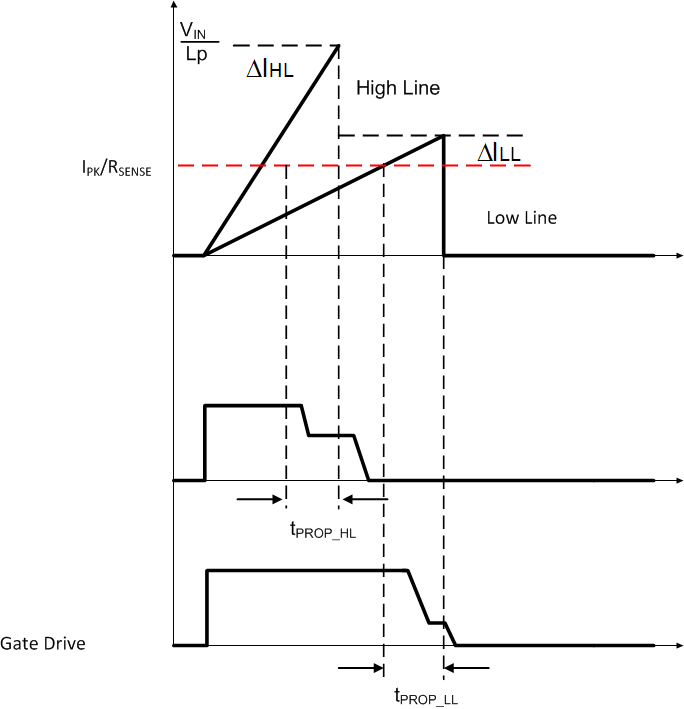 Figure 14. Line-Current Feedforward
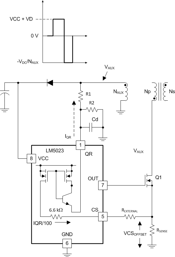
To improve the overpower limit accuracy over the full universal input line, the LM5023 integrates line current limit feedforward. Line current limit feedforward improve the overpower limit by summing a current proportional to the input rectified line into the current sense resistor (RSENSE), refer to Figure 15. The current proportional to the input line biases up the CS pin, this turns off the flyback MOSFET earlier at high input line. This feature compensates for the propagation delays creating a overpower protection that is nearly constant over the universal input line.
To implement line current limit feedforward, the first step is to calculate the QR switching frequency at low line and then at high line when the power supply is operating in current limit.
For this example:
- Lp = 400 µH
- RSENSE = 0.15 Ω
- VDC(min) = 127 V
- VDC(max) = 325 V
- TPROP = 160 ns
- VCS = 0.5 V
- NAUX = 10.9
- NPS = NP/NS = 6
- tDLY = 580 ns


The next step is to calculate the uncompensated output power at the minimum and maximum input line voltage while in current limit.


Step three is to calculate the peak current at high line so it does not deliver more power than while it is operating at low line (94.9 W). One thing that complicates the line current limit feedforward calculation is that with quasi-resonant operation the switching frequency changes with line and load. We have two equations and two unknowns, the peak-primary current and the QR frequency.


Step four is to calculate the peak current.


For the power supply to go into pulse-by-pulse current limit the voltage across the current sense resistor must be 0.5 V.

VCS_OFFSET is the required voltage offset that must be injected across the current sense resistor, RSENSE.

After calculating the required offset voltage, use Equation 41 and Equation 42 to calculate the required current feedforward.
While the main flyback switch is on, Q1, the voltage on the auxiliary winding will be negative and proportional to the rectified line.

IQR should be chosen in the range of 1 mA to 4 mA. The demagnetization circuit impedance should be calculated to limit the maximum current flowing through QR pin to less than 4 mA.
where
- NAUX is the number of turns on the Flyback primary (Np) divided by the number of turns on the transformer Auxiliary (NAUX) winding.
The 6.6-kΩ resistance is internal to the LM5023.
The current mirror in the QR pin input has a gain of 100; this will offset the voltage on the current sense pin shown in Equation 44.

Set IQR = 1.75 mA


No external resistor is required based on the applications describe above, so a 499-Ω resistor and 100-pF capacitor are installed in the CS pin input as a noise filter.
8.2.2.2.1 Overvoltage Protection
Output overvoltage protection is implemented with the LM5023 by monitoring the QR pin during the time when the main flyback MOSFET is off and the energy stored in the transformer primary is being transferred to the secondary. There is a delay prior to sampling the QR pin during the MOSFETs off time, TOVP. There are two reasons for the delay, the first is to blank the voltage spike which is a result of the transformers leakage inductance. The second is to improve the accuracy of the output voltage sensing, referring to the transformer auxiliary winding voltage shown in Figure 11. It is clear there is a down slope in the voltage which represents the decreasing VF of the output rectifier and resistance voltage drop (IS x RS) as the secondary current decreases to zero, so by delaying the sampling of the QR voltage a more accurate representation of the output voltage is achieved.
Connected to the QR pin is a comparator with a 3.0-V reference. The transformers auxiliary voltage is proportional to VOUT by the transformers turns ratio:

To set the OVP, a voltage divider is connected to the transformers auxiliary winding, refer to Figure 14. In Line Current-Limit Feedforward equations were developed to improve the power limit. Resistor R1 was calculated for line current limit feedforward; to implement OVP we now need to calculate R2.


When an OVP fault has been detected, the LM5023 OUT driver is latched-off. VCC will discharge to VCCMIN and the VSD pin will be asserted high, allowing the depletion mode FET to turn-on and charge up the VCC capacitor to VCCON. The VSD pin will be toggled on-off-on to maintain VCC to the controller. The only way to clear the fault is to removed the input power and allow the controllers VCC voltage to drop below VRST, 5.0 V.
8.2.2.3 Valley Switching
For QR operation the flyback MOSFET is turned on with the minimum drain voltage. The delay on the auxiliary winding can be adjusted with an external resistor and capacitor to improve valley switching. The delay-time, tDLY, must equal half of the natural oscillation in Equation 52

By substituting Equation 53.

We can calculate the RC time constant to achieve the minimum drain voltage when the LM5023 turns on the Flyback MOSFET.

The LM5023 QR pin’s capacitance is approximately 20 pF, so CdUSED = Cd –20 pF

R1 and R2 were previously calculated to set the line current limit feedforward and overvoltage protection.
8.2.2.4 Hiccup Mode
Hiccup Mode is a method to prevent the power supply from over-heating during and extended overload condition. In an overload fault, the current limit comparator turns off the driver output on pulse-by-pulse basis. This starts the over load detection timer, after the over load detection timer (OLDT) times out, the current limit comparator is rechecked, if the power supply is still in an overload condition, the OUT drive is latched-off and VCC is allowed to drop to VCCOFF (7.5 V).
When VCC reaches VCCOFF, the VSD open drain output is disabled allowing the depletion mode start-up FET to turn-on, charging up the VCC capacitor to VCCON (12.5 V). When VCC reaches VCCON, the VSD output goes low turning-off the depletion mode FET. The VCC capacitor is discharged from VCCON to VCCOFF at a rate proportional to the VCC capacitor and the ICCST current (340-µA typical). The charging and discharging of the VCC capacitor is repeated four times (refer to Figure 16) use Equation 56 to figure the total Hiccup time.

After allowing VCC to charge and discharge four times, the LM5023 goes through an auto restart sequence, enabling the LM5023 soft-start and driver output. It is important to set the over load detection timer long enough so that under low input-line and full-load conditions that the power supply will have enough time to start-up.
The over load detection timer can be set with the resister in series with the VSD pin VSD), refer to Figure 8.


Normally it is recommended that RVSD > 1 MΩ, if a lower value is used then the standby power will be higher.
Assuming the depletion mode FET charges the VCC capacitor with 2 mA, VCC capacitor is 10 µF.


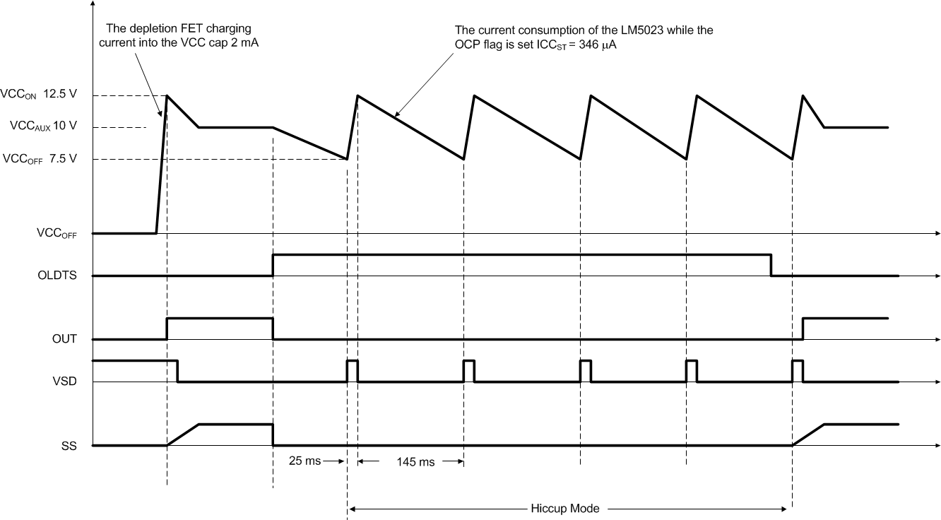 Figure 16. Hiccup Mode Timing
8.2.3 Application Curves
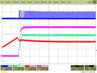
| CH1: OUT, 10 V/div | CH2: SS, 2 V/div |
| CH3: VCC, 5 V/div | CH4: VOUT, 5 V/div |
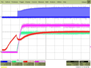
| CH1: OUT, 10 V/div | CH2: SS, 2 V/div |
| CH3: VCC, 5 V/div | CH4: VOUT, 5 V/div |
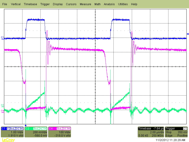
| CH1: OUT, 10 V/div | CH2: CS, 200 mV/div | ||
| CH4: VDS, 100 V/div |
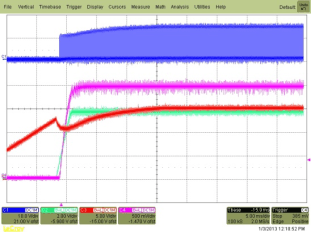
| CH1: OUT, 10 V/div | CH2: SS, 2 V/div |
| CH3: VCC, 5 V/div | CH4: VOUT, 5 V/div |
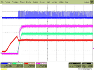
| CH1: OUT, 10 V/div | CH2: SS, 2 V/div |
| CH3: VCC, 5 V/div | CH4: VOUT, 5 V/div |
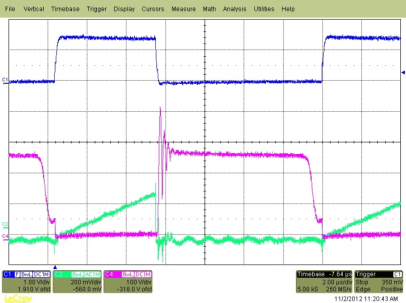
| CH1: OUT, 10 V/div | CH2: CS, 200 mV/div |
| CH4: VDS, 100 V/div |

