ZHCSQ27 October 2022 LM5012
PRODUCTION DATA
- 1 特性
- 2 应用
- 3 说明
- 4 Revision History
- 5 Device Comparison Table
- 6 Pin Configuration and Functions
- 7 Specifications
-
8 Detailed Description
- 8.1 Overview
- 8.2 Functional Block Diagram
- 8.3
Feature Description
- 8.3.1 Control Architecture
- 8.3.2 Internal VCC Regulator and Bootstrap Capacitor
- 8.3.3 Regulation Comparator
- 8.3.4 Internal Soft Start
- 8.3.5 On-Time Generator
- 8.3.6 Current Limit
- 8.3.7 N-Channel Buck Switch and Driver
- 8.3.8 Schottky Diode Selection
- 8.3.9 Enable and Undervoltage Lockout (EN/UVLO)
- 8.3.10 Power Good (PGOOD)
- 8.3.11 Thermal Protection
- 8.4 Device Functional Modes
- 9 Application and Implementation
- 10Device and Documentation Support
- 11Mechanical, Packaging, and Orderable Information
9.4.2.1 Thermal Considerations
As with any power conversion device, the LM5012 dissipates internal power while operating. The effect of this power dissipation is to raise the internal temperature of the converter above ambient. The internal die temperature (TJ) is a function of the following:
- Ambient temperature
- Power loss
- Effective thermal resistance, RθJA, of the device
- PCB combination
The maximum internal die temperature for the LM5012 must be limited to 150°C. This limit establishes a limit on the maximum device power dissipation and, therefore, the load current. Equation 20 shows the relationships between the important parameters. It is easy to see that larger ambient temperatures (TA) and larger values of RθJA reduce the maximum available output current. The converter efficiency can be estimated by using the curves provided in this data sheet. Note that these curves include the power loss in the inductor. If the desired operating conditions cannot be found in one of the curves, then interpolation can be used to estimate the efficiency. Alternatively, the EVM can be adjusted to match the desired application requirements and the efficiency can be measured directly. The correct value of RθJA is more difficult to estimate. As stated in the Semiconductor and IC Package Thermal Metrics application report, the value of RθJA given in the Thermal Information is not valid for design purposes and must not be used to estimate the thermal performance of the application. The values reported in that table were measured under a specific set of conditions that are rarely obtained in an actual application. The data given for RθJC(bott) and ΨJT can be useful when determining thermal performance. See the Semiconductor and IC Package Thermal Metrics application report for more information and the resources given at the end of this section.
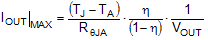
where
- η is efficiency.
The effective RθJA is a critical parameter and depends on many factors such as the following:
- Power dissipation
- Air temperature/flow
- PCB area
- Copper heat-sink area
- Number of thermal vias under the package
- Adjacent component placement
The LM5012 features a die attach paddle, or "thermal pad" (EP), to provide a place to solder down to the PCB heat-sinking copper. This feature provides a good heat conduction path from the regulator junction to the heat sink and must be properly soldered to the PCB heat sink copper. Typical examples of RΘJA can be found in Figure 9-15. The copper area given in the graph is for each layer. The top and bottom layers are 2-oz. copper each, while the inner layers are 1 oz. Remember that the data given in this graph is for illustration purposes only, and the actual performance in any given application depends on all of the previously mentioned factors.
To continue with the design example, assume that the user has an ambient temperature of 70ºC and wishes to estimate the required copper area to keep the device junction temperature below 125ºC, at full load. From the curves in Figure 9-3, an efficiency of about 92% was found at an input voltage of 48 V with output of 12 V with 1.75-A load. The efficiency is somewhat less at high junction temperatures, so an efficiency of approximately 90% is assumed. This gives a total loss of about 2.3 W. Subtracting out the conduction loss alone for the inductor and catch diode, the user arrives at a device dissipation of about 1.54 W. With this information, the user can calculate the required RθJA of about 30ºC/W. Based on Figure 9-15, the required copper area is about 40 cm2, for a two-layer PCB.
Engineering best judgment is to be used if using a lossy inductor, diode, or both, in the application, as their large losses may contribute to localized heating of the component, as well, the nearby regulator. As an example, biasing the Schottky diode (DSW) with 1.3-A continuous current (average current for 1.75-A load current) results in approximately 10°C rise in the case temperature of the regulator. This must be "buffered" for in the ambient temperature used in the previous calculation. For more details on these calculations, please see the PCB Thermal Design Tips for Automotive DC/DC Converters application report.
The following resources can be used as a guide to optimal thermal PCB design and estimating RθJA for a given application environment:
- Semiconductor and IC Package Thermal Metrics application report
- AN-2020 Thermal Design By Insight, Not Hindsight application report
- A Guide to Board Layout for Best Thermal Resistance for Exposed Pad Packages application report
- Using New Thermal Metrics application report
- PCB Thermal Design Tips for Automotive DC/DC Converters application report