SNVS307G September 2004 – April 2016 LM5010
PRODUCTION DATA.
- 1 Features
- 2 Applications
- 3 Description
- 4 Revision History
- 5 Pin Configuration and Functions
- 6 Specifications
- 7 Detailed Description
- 8 Application and Implementation
- 9 Power Supply Recommendations
- 10Layout
- 11Device and Documentation Support
- 12Mechanical, Packaging, and Orderable Information
封装选项
机械数据 (封装 | 引脚)
散热焊盘机械数据 (封装 | 引脚)
订购信息
7 Detailed Description
7.1 Overview
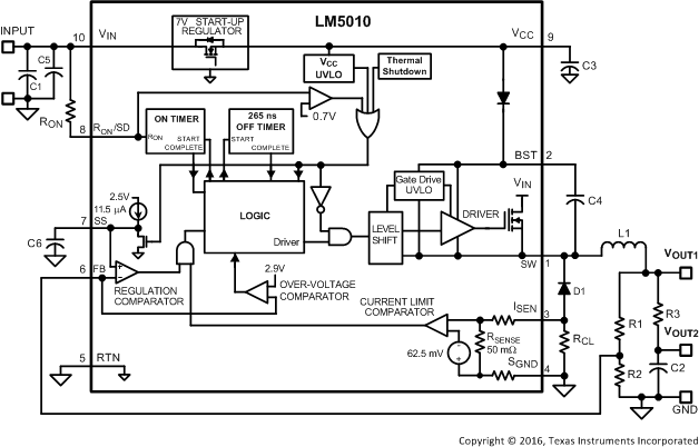
The LM5010 step-down switching regulator features all the functions needed to implement a low-cost, efficient, buck bias power converter. This high-voltage regulator contains a 75-V N-channel buck switch, is easy to implement, and is provided in HTSSOP and thermally-enhanced, WSON packages. The regulator is based on a control scheme using an ON-time inversely proportional to VIN. The control scheme requires no loop compensation. The functional block diagram of the LM5010 is shown in the Functional Block Diagram.
The LM5010 can be applied in numerous applications to efficiently regulate down higher voltages. This regulator is well-suited for 48-V telecom and 42-V automotive power bus ranges. Additional features include: thermal shutdown, VCC undervoltage lockout, gate drive undervoltage lockout, maximum duty cycle limit timer, and the valley current limit functionality.
7.2 Functional Block Diagram
7.3 Feature Description
The LM5010 step-down switching regulator features all the functions needed to implement a low-cost, efficient buck bias power converter capable of supplying in excess of 1 A to the load. This high voltage regulator contains an N-Channel buck switch, is easy to implement, and is available in the thermally enhanced 10-pin WSON and 14-pin HTSSOP packages. The regulator’s operation is based on a constant ON-time control scheme, where the ON-time varies inversely with VIN. This feature results in the operating frequency remaining relatively constant with load and input voltage variations. The switching frequency can range from 100 kHz to > 1 MHz. The hysteretic control requires no loop compensation, resulting in very fast load transient response. The valley current limit detection circuit, internally set at 1.25 A, holds the buck switch off until the high current level subsides. The LM5010 can be applied in numerous applications to efficiently regulate down higher voltages. This regulator is well suited for 48-V telecom applications, as well as the new 42-V automotive power bus. Implemented as a point-of-load regulator following a highly-efficient intermediate bus converter can result in high overall system efficiency. Features include: Thermal shutdown, VCC undervoltage lockout, gate drive undervoltage lockout, and maximum duty cycle limit.
7.3.1 Control Circuit Overview
The LM5010 buck DC-DC regulator employs a control scheme based on a comparator and a one-shot ON timer, with the output voltage feedback (FB) compared to an internal reference (2.5 V). If the FB voltage is below the reference the buck switch is turned on for a time period determined by the input voltage and a programming resistor (RON). Following the ON-time the switch remains off for 265 ns, or until the FB voltage falls below the reference, whichever is longer. The buck switch then turns on for another ON-time period. Typically when the load current increases suddenly, the OFF-times are temporarily at the minimum of 265 ns. Once regulation is established, the OFF-time resumes its normal value. The output voltage is set by two external resistors (R1, R2). The regulated output voltage is calculated with Equation 1.
Output voltage regulation is based on ripple voltage at the feedback input, requiring a minimum amount of ESR for the output capacitor C2. The LM5010 requires a minimum of 25-mV of ripple voltage at the FB pin. In cases where the capacitor’s ESR is insufficient, additional series resistance may be required (R3 in Functional Block Diagram).
When in regulation, the LM5010 operates in continuous conduction mode at heavy load currents and discontinuous conduction mode at light load currents. In continuous conduction mode current always flows through the inductor, never reaching zero during the OFF-time. In this mode the operating frequency remains relatively constant with load and line variations. The minimum load current for continuous conduction mode is one-half the inductor’s ripple current amplitude. Calculate the approximate operating frequency with Equation 2.

The buck switch duty cycle is approximately equal to Equation 3.

At low load current, the circuit operates in discontinuous conduction mode, during which the inductor current ramps up from zero to a peak during the ON-time, then ramps back to zero before the end of the OFF-time. The next ON-time period starts when the voltage at FB falls below the reference until then the inductor current remains zero, and the load current is supplied by the output capacitor (C2). In this mode the operating frequency is lower than in continuous conduction mode, and varies with load current. Conversion efficiency is maintained at light loads because the switching losses reduce with the reduction in load and frequency. Calculate the approximate discontinuous operating frequency with Equation 4.

where
- RL = the load resistance
For applications where lower output voltage ripple is required, the output can be taken directly from a low ESR output capacitor as shown in Figure 8. However, R3 slightly degrades the load regulation.
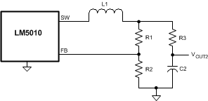 Figure 8. Low Ripple Output Configuration
7.3.2 Start-Up Regulator (VCC)
The start-up regulator is integral to the LM5010. The input pin (VIN) can be connected directly to line voltages up to 75 V. The VCC output is regulated at 7 V, ±6%, and is current-limited to 10 mA. Upon power up the regulator sources current into the external capacitor at VCC (C3). With a 0.1-µF capacitor at VCC, approximately 58 µs are required for the VCC voltage to reach the undervoltage lockout threshold (UVLO) of 5.8 V (t1 in Figure 7), at which time the buck switch is enabled, and the soft-start pin is released to allow the soft-start capacitor (C6) to charge up. VOUT then increases to its regulated value as the soft-start voltage increases (t2 in Figure 7).
The minimum input operating voltage is determined by the regulator’s dropout voltage, the VCC UVLO falling threshold (≊5.65 V), and the frequency. When VCC falls below the falling threshold the VCC UVLO activates to shut off the buck switch and ground the soft-start pin. If VCC is externally loaded, the minimum input voltage increases since the output impedance at VCC is ≊140 Ω at low VIN. See Figure 1 and Figure 2. In applications involving a high value for VIN where power dissipation in the start-up regulator is a concern, an auxiliary voltage can be diode connected to the VCC pin (Figure 9). Setting the auxiliary voltage to between 7.5 V and 14 V shuts off the internal regulator, reducing internal power dissipation. Figure 3 shows the current required into the VCC pin. A diode connects VCC to VIN internally.
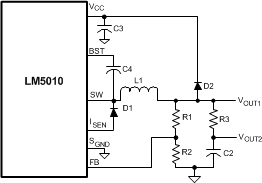 Figure 9. Self Biased Configuration
7.3.3 Regulation Comparator
The feedback voltage at FB is compared to the voltage at the soft-start pin (2.5 V, ±2%). In normal operation (the output voltage is regulated) an ON-time period is initiated when the voltage at FB falls below 2.5 V. The buck switch stays on for the ON-time causing the FB voltage to rise above 2.5 V. After the ON-time period the buck switch stays off until the FB voltage falls below 2.5 V. Bias current at the FB pin is less than 5 nA over temperature.
7.3.4 Overvoltage Comparator
The feedback voltage at FB is compared to an internal 2.9-V reference. If the voltage at FB rises above 2.9 V, the ON-time is immediately terminated. This condition can occur if the input voltage or the output load changes suddenly. The buck switch will not turn on again until the voltage at FB falls below 2.5 V.
7.3.5 ON-Time Control
The ON-time of the internal switch (see Figure 4) is determined by the RON resistor and the input voltage (VIN), calculated with Equation 5.

The inverse relationship of tON vs VIN results in a nearly constant frequency as VIN is varied. If the application requires a high frequency, the minimum value for tON, and consequently RON, is limited by the OFF-time (265 ns, ±15%) which limits the maximum duty cycle at minimum VIN. The tolerance for Equation 5 is ±25%. Frequencies in excess of 1 MHz are possible with the LM5010.
7.3.6 Current Limit
Current limit detection occurs during the OFF-time by monitoring the recirculating current through the free-wheeling diode (D1). The detection threshold is 1.25 A, ±0.25 A. Referring to Functional Block Diagram, when the buck switch is off the inductor current flows through the load, into SGND, through the sense resistor, out of ISEN and through D1. If that current exceeds the threshold the current limit comparator output switches to delay the start of the next ON-time period. The next ON-time starts when the current out of ISEN is below the threshold and the voltage at FB is below 2.5 V. If the overload condition persists causing the inductor current to exceed the threshold during each ON-time, that is detected at the beginning of each OFF-time. The operating frequency is lower due to longer-than-normal OFF-times.
Figure 10 illustrates the inductor current waveform. During normal operation the load current is IO, the average of the ripple waveform. When the load resistance decreases the current ratchets up until the lower peak attempts to exceed the threshold. During the Current Limited portion of Figure 10, the current ramps down to the threshold during each OFF-time, initiating the next ON-time (assuming the voltage at FB is < 2.5 V). During each ON-time the current ramps up an amount equal to Equation 6.

During this time the LM5010 is in a constant current mode, with an average load current (IOCL) equal to the threshold + ΔI / 2.
The valley current limit technique allows the load current to exceed the current limit threshold as long as the lower peak of the inductor current is less than the threshold.
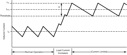 Figure 10. Inductor Current, Current Limit Operation
The current limit threshold can be increased by connecting an external resistor (RCL) between SGND and ISEN. The external resistor typically is less than 1 Ω, and its calculation is explained in Application and Implementation.
The peak current out of SW and ISEN must not exceed 3.5 A. The average current out of SW must be less than
3 A, and the average current out of ISEN must be less than 2 A.
7.3.7 Soft Start
The soft-start feature allows the converter to gradually reach a steady-state operating point, thereby reducing start-up stresses and current surges. Upon turnon, after VCC reaches the undervoltage threshold (t1 in Figure 7), an internal 11.5-µA current source charges the external capacitor at the soft-start pin to 2.5 V (t2 in Figure 7). The ramping voltage at SS (and at the non-inverting input of the regulation comparator) ramps up the output voltage in a controlled manner. This feature keeps the load current from going to current limit during start-up, thereby reducing inrush currents.
An internal switch grounds the soft-start pin if VCC is below the undervoltage lockout threshold, if a thermal shutdown occurs, or if the circuit is shutdown using the RON/SD pin.
7.3.8 N-Channel Buck Switch and Driver
The LM5010 integrates an N-Channel buck switch and associated floating high voltage gate driver. The peak current through the buck switch must not be allowed to exceed 3.5 A, and the average current must be less than 3 A. The gate driver circuit is powered by the external bootstrap capacitor between BST and SW (C4). During each OFF-time, the SW pin is at approximately –1 V, and C4 is recharged from VCC through the internal high voltage diode. The minimum OFF-time of 265 ns ensures a minimum time each cycle to recharge the bootstrap capacitor. TI recommends a 0.022-µF ceramic capacitor for C4.
7.3.9 Thermal Shutdown
The LM5010 should be operated so the junction temperature does not exceed 125°C. If the junction temperature increases above that, an internal Thermal Shutdown circuit activates (typically) at 175°C, taking the controller to a low-power reset state by disabling the buck switch and the ON timer, and grounding the soft-start pin. This feature helps prevent catastrophic failures from accidental device overheating. When the junction temperature reduces below 155°C (typical hysteresis = 20°C), the softstart pin is released and normal operation resumes.
7.4 Device Functional Modes
7.4.1 Shutdown
The LM5010 can be remotely shut down by taking the RON/SD pin below 0.65 V. See Figure 11. In this mode the soft-start pin is internally grounded, the ON timer is disabled, and the input current at VIN is reduced (Figure 6). Releasing the RON/SD pin allows normal operation to resume. When the switch is open, the nominal voltage at RON/SD is shown in Figure 5.
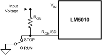 Figure 11. Shutdown Implementation