ZHCSNT4I February 2006 – May 2021 LM5009
PRODUCTION DATA
- 1 特性
- 2 应用
- 3 说明
- 4 Revision History
- 5 Pin Configuration and Functions
- 6 Specifications
- 7 Detailed Description
-
8 Application and Implementation
- 8.1 Application Information
- 8.2
Typical Application
- 8.2.1 Design Requirements
- 8.2.2
Detailed Design Procedure
- 8.2.2.1 Output Resistor Divider Selection
- 8.2.2.2 Frequency Selection
- 8.2.2.3 Inductor Selection
- 8.2.2.4 VCC and Bootstrap Capacitor
- 8.2.2.5 Output Capacitor Selection
- 8.2.2.6 Current Limit Off-Timer Setting
- 8.2.2.7 Rectifier Diode Selection
- 8.2.2.8 Input Capacitor Selection
- 8.2.2.9 Ripple Configuration
- 8.2.3 Application Curves
- 8.3 Do's and Don'ts
- 9 Power Supply Recommendations
- 10Layout
- 11Device and Documentation Support
- 12Mechanical, Packaging, and Orderable Information
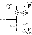
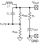
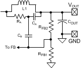
8.2.2.9 Ripple Configuration
The LM5009 uses a constant-on-time (COT) control scheme where the on-time is terminated by a one-shot and the off-time is terminated by the feedback voltage (VFB) falling below the reference voltage. Therefore, for stable operation, the feedback voltage must decrease monotonically in phase with the inductor current during the off-time. Furthermore, this change in feedback voltage (VFB) during off-time must be large enough to dominate any noise present at the feedback node.
Table 8-2 presents three different methods for generating appropriate voltage ripple at the feedback node. Type 1 and type 2 ripple circuits couple the ripple from the output of the converter to the feedback node (FB). The output voltage ripple has two components:
- Capacitive ripple caused by the inductor current ripple charging or discharging the output capacitor.
- Resistive ripple caused by the inductor current ripple flowing through the ESR of the output capacitor and R3.
| TYPE 1 | TYPE 2 | TYPE 3 |
|---|---|---|
| Lowest cost | Reduced ripple | Minimum ripple |
 |  |  |
Equation 12. 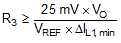 | Equation 13. 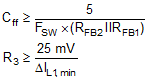 | Equation 14. 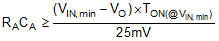 |
The capacitive ripple is out of phase with the inductor current. As a result, the capacitive ripple does not decrease monotonically during the off-time. The resistive ripple is in phase with the inductor current and decreases monotonically during the off-time. The resistive ripple must exceed the capacitive ripple at output (VOUT) for stable operation. If this condition is not satisfied, then unstable switching behavior is observed in COT converters with multiple on-time bursts in close succession followed by a long off-time.
The type 3 ripple method uses a ripple injection circuit with RA, CA, and the switch node (SW) voltage to generate a triangular ramp. This triangular ramp is then ac-coupled into the feedback node (FB) using the capacitor CB. This circuit is suited for applications where low output voltage ripple is imperative because this circuit does not use the output voltage ripple. See application note AN-1481 Controlling Output Ripple and Achieving ESR Independence in Constant On-Time (COT) Regulator Designs, SNVA166 for more details on each ripple generation method.