ZHCSIX0H March 2009 – October 2018 LM5008A
PRODUCTION DATA.
7.3.2 Start-Up Regulator (VCC)
The high voltage bias regulator is integrated within the LM5008A. The input pin (VIN) can be connected directly to line voltages between 6 V and 95 V, with transient capability to 100 V. Referring to the Functional Block Diagram and Figure 2, when VIN is between 6 V and the bypass threshold (nominally 8.5 V), the bypass switch (Q2) is on, and VCC tracks VIN within 100 mV to 150 mV. The bypass switch on-resistance is approximately 100 Ω, with inherent current limiting at approximately 100 mA. When VIN is above the bypass threshold Q2 is turned off, and VCC is regulated at 7 V. The VCC regulator output current is limited at approximately 9.2 mA. When the LM5008A is shut down using the RT/SD pin, the VCC bypass switch is shut off regardless of the voltage at VIN.
When VIN exceeds the bypass threshold, the time required for Q2 to shut off is approximately 2 µs to 3 µs. The capacitor at VCC (C3) must be a minimum of 0.47 µF to prevent the voltage at VCC from rising above its absolute maximum rating in response to a step input applied at VIN. C3 must be placed as close as possible to the VCC and RTN pins. In applications with a relatively high input voltage, power dissipation in the bias regulator is a concern. An auxiliary voltage of between 7.5 V and 14 V can be diode connected to the VCC pin to shut off the VCC regulator, thereby reducing internal power dissipation. The current required into the VCC pin is shown in Figure 6. Internally a diode connects VCC to VIN requiring that the auxiliary voltage be less than VIN.
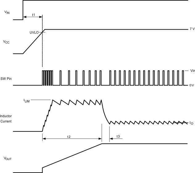
The turnon sequence is shown in Figure 8. During the initial delay (t1), VCC ramps up at a rate determined by its current limit and C3 while internal circuitry stabilizes. When VCC reaches the upper threshold of its undervoltage lockout (UVLO, typically 5.3 V), the buck switch is enabled. The inductor current increases to the current limit threshold (ILIM), and during t2 the VOUT increases as the output capacitor charges up. When VOUT reaches the intended voltage the average inductor current decreases (t3) to the nominal load current (IO).
 Figure 8. Start-Up Sequence