SNVS656D September 2010 – October 2016 LM3492 , LM3492-Q1
PRODUCTION DATA.
- 1 Features
- 2 Applications
- 3 Description
- 4 Revision History
- 5 Description (continued)
- 6 Pin Configuration and Functions
- 7 Specifications
-
8 Detailed Description
- 8.1 Overview
- 8.2 Functional Block Diagram
- 8.3 Feature Description
- 8.4 Device Functional Modes
- 8.5 Programming
- 9 Application and Implementation
- 10Power Supply Recommendations
- 11Layout
- 12Device and Documentation Support
- 13Mechanical, Packaging, and Orderable Information
1 Features
-
Boost Converter:
- LM3492-Q1 is an Automotive Grade Product That is AEC Q100 Grade 1 Qualified
- Very Wide Input Voltage Ranged
From 4.5 V to 65 V - Programmable Soft Start
- No Loop Compensation Required
- Stable With Ceramic and Other Low ESR Capacitors With No Audible Noise
- Nearly Constant Switching Frequency Programmable From 200 kHz to 1 MHz
-
Current Regulators:
- Programmable LED Current from 50 mA to 200 mA
- 1000:1 Contrast Ratio at a Dimming Frequency of More Than 3 kHz, Minimum LED Current Pulse Width is 300 ns
- Two Individual Dimmable LED Strings up to
65 V, Total 15 W (Typically 28 LEDs at
150 mA) - Dynamic Headroom Control Maximizes Efficiency
- Over-Power Protection
- ±3% Current Accuracy
-
Supervisory Functions:
- Precision Enable
- COMM I/O Pin for Diagnostic and Commands
- Thermal Shutdown Protection
- Thermally Enhanced 20-Pin HTSSOP package
2 Applications
- Ultra-High Contrast Ratio 6.5”-10” LCD Display Backlight up to 28 LEDs
- Automotive or Marine GPS Displays
3 Description
The LM3492/-Q1 integrates a boost converter and a two-channel current regulator to implement a high efficient and cost effective LED driver for driving two individually dimmable LED strings with a maximum power of 15 W and an output voltage of up to 65 V. The boost converter employs a proprietary Projected-On-Time control method to give a fast transient response with no compensation required, and a nearly constant switching frequency programmable from 200 kHz to 1 MHz. The application circuit is stable with ceramic capacitors and produces no audible noise on dimming. The programmable peak current limit and soft-start features reduce current surges at start-up, and an integrated 190 mΩ, 3.9-A N-Channel MOSFET switch minimizes the solution size.
Device Information(1)
| PART NUMBER | PACKAGE | BODY SIZE (NOM) |
|---|---|---|
| LM3492 | HTSSOP (20) | 7.80 mm × 4.40 mm |
| LM3492-Q1 |
- For all available packages, see the orderable addendum at the end of the data sheet.
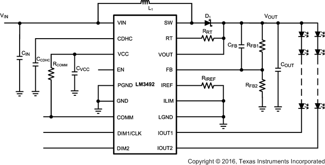
Typical Application
