SNVS616H April 2009 – July 2015 LM3429 , LM3429-Q1
PRODUCTION DATA.
- 1 Features
- 2 Applications
- 3 Description
- 4 Revision History
- 5 Pin Configuration and Functions
- 6 Specifications
-
7 Detailed Description
- 7.1 Overview
- 7.2 Functional Block Diagram
- 7.3
Feature Description
- 7.3.1 Current Regulators
- 7.3.2 Predictive Off-Time (PRO) Control
- 7.3.3 Switching Frequency
- 7.3.4 Average LED Current
- 7.3.5 Analog Dimming
- 7.3.6 Current Sense and Current Limit
- 7.3.7 Control Loop Compensation
- 7.3.8 Output Overvoltage Lockout (OVLO)
- 7.3.9 Input Undervoltage Lockout (UVLO)
- 7.3.10 PWM Dimming
- 7.3.11 Startup Regulator (VCC LDO)
- 7.3.12 Thermal Shutdown
- 7.4 Device Functional Modes
-
8 Application and Implementation
- 8.1 Application Information
- 8.2
Typical Applications
- 8.2.1
Basic Topology Schematics
- 8.2.1.1 Design Requirements
- 8.2.1.2
Detailed Design Procedure
- 8.2.1.2.1 Operating Point
- 8.2.1.2.2 Switching Frequency
- 8.2.1.2.3 Average LED Current
- 8.2.1.2.4 Inductor Ripple Current
- 8.2.1.2.5 LED Ripple Current
- 8.2.1.2.6 Peak Current Limit
- 8.2.1.2.7 Loop Compensation
- 8.2.1.2.8 Input Capacitance
- 8.2.1.2.9 NFET
- 8.2.1.2.10 Diode
- 8.2.1.2.11 Output OVLO
- 8.2.1.2.12 Input UVLO
- 8.2.1.2.13 PWM Dimming Method
- 8.2.1.2.14 Analog Dimming Method
- 8.2.2
Buck-Boost Application - 6 LEDs at 1 A
- 8.2.2.1 Design Requirements
- 8.2.2.2
Detailed Design Procedure
- 8.2.2.2.1 Operating Point
- 8.2.2.2.2 Switching Frequency
- 8.2.2.2.3 Average LED Current
- 8.2.2.2.4 Inductor Ripple Current
- 8.2.2.2.5 Output Capacitance
- 8.2.2.2.6 Peak Current Limit
- 8.2.2.2.7 Loop Compensation
- 8.2.2.2.8 Input Capacitance
- 8.2.2.2.9 NFET
- 8.2.2.2.10 Diode
- 8.2.2.2.11 Input UVLO
- 8.2.2.2.12 Output OVLO
- 8.2.2.3 Application Curve
- 8.2.3 Boost PWM Dimming Application - 9 LEDs at 1 A
- 8.2.4 Buck-Boost Analog Dimming Application - 4 LEDs at 2A
- 8.2.5 Boost Analog Dimming Application - 12 LEDs at 700 mA
- 8.2.6 Buck-Boost PWM Dimming Application - 6 LEDs at 500 mA
- 8.2.7 Buck Application - 3 LEDS at 1.25 A
- 8.2.8 Buck-Boost Thermal Foldback Application - 8 LEDs at 2.5 A
- 8.2.9 SEPIC Application - 5 LEDs at 750 mA
- 8.2.1
Basic Topology Schematics
- 9 Power Supply Recommendations
- 10Layout
- 11Device and Documentation Support
- 12Mechanical, Packaging, and Orderable Information
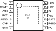
5 Pin Configuration and Functions
PWP Package
14- Pin HTSSOP
Top View

Pin Functions
| PIN | I/O | DESCRIPTION | APPLICATION INFORMATION | |
|---|---|---|---|---|
| NO. | NAME | |||
| 1 | VIN | I | Input Voltage | Bypass with 100 nF capacitor to AGND as close to the device as possible in the circuit board layout. |
| 2 | COMP | I | Compensation | Connect a capacitor to AGND to set compensation. |
| 3 | CSH | I | Current Sense High | Connect a resistor to AGND to set signal current. For analog dimming, connect current source or potentiometer to AGND (see Analog Dimming section). |
| 4 | RCT | I | Resistor Capacitor Timing | Connect a resistor from the switch node and a capacitor to AGND to set the switching frequency. |
| 5 | AGND | GND | Analog Ground | Connect to PGND through the DAP copper circuit board pad to provide proper ground return for CSH, COMP, and RCT. |
| 6 | OVP | I | Overvoltage Protection | Connect to a resistor divider from the output (VO) or the input to program output overvoltage lockout (OVLO). Turn-off threshold is 1.24 V and hysteresis for turn-on is provided by 20 µA current source. |
| 7 | nDIM | I | Not DIM input | Connect a PWM signal for dimming as detailed in the PWM Dimming section and/or a resistor divider from VIN to program input undervoltage lockout (UVLO). Turn-on threshold is 1.24 V and hysteresis for turn-off is provided by 20 µA current source. |
| 8 | NC | No Connection | Leave open. | |
| 9 | PGND | GND | Power Ground | Connect to AGND through DAP copper pad to provide ground return for GATE. |
| 10 | GATE | O | Gate Drive Output | Connect to the gate of the external NFET. |
| 11 | VCC | I | Internal Regulator Output | Bypass with a 2.2 µF–3.3 µF, ceramic capacitor to PGND. |
| 12 | IS | I | Main Switch Current Sense | Connect to the drain of the main N-channel MosFET switch for RDS-ON sensing or to a sense resistor installed in the source of the same device. |
| 13 | HSP | I | LED Current Sense Positive | Connect through a series resistor to LED current sense resistor (positive). |
| 14 | HSN | I | LED Current Sense Negative | Connect through a series resistor to LED current sense resistor (negative). |
| DAP (15) | DAP | GND | Thermal pad on bottom of IC | Connect to AGND and PGND. |