SNVS616H April 2009 – July 2015 LM3429 , LM3429-Q1
PRODUCTION DATA.
- 1 Features
- 2 Applications
- 3 Description
- 4 Revision History
- 5 Pin Configuration and Functions
- 6 Specifications
-
7 Detailed Description
- 7.1 Overview
- 7.2 Functional Block Diagram
- 7.3
Feature Description
- 7.3.1 Current Regulators
- 7.3.2 Predictive Off-Time (PRO) Control
- 7.3.3 Switching Frequency
- 7.3.4 Average LED Current
- 7.3.5 Analog Dimming
- 7.3.6 Current Sense and Current Limit
- 7.3.7 Control Loop Compensation
- 7.3.8 Output Overvoltage Lockout (OVLO)
- 7.3.9 Input Undervoltage Lockout (UVLO)
- 7.3.10 PWM Dimming
- 7.3.11 Startup Regulator (VCC LDO)
- 7.3.12 Thermal Shutdown
- 7.4 Device Functional Modes
-
8 Application and Implementation
- 8.1 Application Information
- 8.2
Typical Applications
- 8.2.1
Basic Topology Schematics
- 8.2.1.1 Design Requirements
- 8.2.1.2
Detailed Design Procedure
- 8.2.1.2.1 Operating Point
- 8.2.1.2.2 Switching Frequency
- 8.2.1.2.3 Average LED Current
- 8.2.1.2.4 Inductor Ripple Current
- 8.2.1.2.5 LED Ripple Current
- 8.2.1.2.6 Peak Current Limit
- 8.2.1.2.7 Loop Compensation
- 8.2.1.2.8 Input Capacitance
- 8.2.1.2.9 NFET
- 8.2.1.2.10 Diode
- 8.2.1.2.11 Output OVLO
- 8.2.1.2.12 Input UVLO
- 8.2.1.2.13 PWM Dimming Method
- 8.2.1.2.14 Analog Dimming Method
- 8.2.2
Buck-Boost Application - 6 LEDs at 1 A
- 8.2.2.1 Design Requirements
- 8.2.2.2
Detailed Design Procedure
- 8.2.2.2.1 Operating Point
- 8.2.2.2.2 Switching Frequency
- 8.2.2.2.3 Average LED Current
- 8.2.2.2.4 Inductor Ripple Current
- 8.2.2.2.5 Output Capacitance
- 8.2.2.2.6 Peak Current Limit
- 8.2.2.2.7 Loop Compensation
- 8.2.2.2.8 Input Capacitance
- 8.2.2.2.9 NFET
- 8.2.2.2.10 Diode
- 8.2.2.2.11 Input UVLO
- 8.2.2.2.12 Output OVLO
- 8.2.2.3 Application Curve
- 8.2.3 Boost PWM Dimming Application - 9 LEDs at 1 A
- 8.2.4 Buck-Boost Analog Dimming Application - 4 LEDs at 2A
- 8.2.5 Boost Analog Dimming Application - 12 LEDs at 700 mA
- 8.2.6 Buck-Boost PWM Dimming Application - 6 LEDs at 500 mA
- 8.2.7 Buck Application - 3 LEDS at 1.25 A
- 8.2.8 Buck-Boost Thermal Foldback Application - 8 LEDs at 2.5 A
- 8.2.9 SEPIC Application - 5 LEDs at 750 mA
- 8.2.1
Basic Topology Schematics
- 9 Power Supply Recommendations
- 10Layout
- 11Device and Documentation Support
- 12Mechanical, Packaging, and Orderable Information
8 Application and Implementation
NOTE
Information in the following applications sections is not part of the TI component specification, and TI does not warrant its accuracy or completeness. TI’s customers are responsible for determining suitability of components for their purposes. Customers should validate and test their design implementation to confirm system functionality.
8.1 Application Information
8.1.1 Inductor
The inductor (L1) is the main energy storage device in a switching regulator. Depending on the topology, energy is stored in the inductor and transfered to the load in different ways (as an example, buck-boost operation is detailed in the Current Regulators section). The size of the inductor, the voltage across it, and the length of the switching subinterval (tON or tOFF) determines the inductor current ripple (ΔiL-PP). In the design process, L1 is chosen to provide a desired ΔiL-PP. For a buck regulator the inductor has a direct connection to the load, which is good for a current regulator. This requires little to no output capacitance therefore ΔiL-PP is basically equal to the LED ripple current ΔiLED-PP. However, for boost and buck-boost regulators, there is always an output capacitor which reduces ΔiLED-PP, therefore the inductor ripple can be larger than in the buck regulator case where output capacitance is minimal or completely absent.
In general, ΔiLED-PP is recommended by manufacturers to be less than 40% of the average LED current (ILED). Therefore, for the buck regulator with no output capacitance, ΔiL-PP should also be less than 40% of ILED. For the boost and buck-boost topologies, ΔiL-PP can be much higher depending on the output capacitance value. However, ΔiL-PP is suggested to be less than 100% of the average inductor current (IL) to limit the RMS inductor current.
L1 is also suggested to have an RMS current rating at least 25% higher than the calculated minimum allowable RMS inductor current (IL-RMS).
8.1.2 LED Dynamic Resistance (rD)
When the load is a string of LEDs, the output load resistance is the LED string dynamic resistance plus RSNS. LEDs are PN junction diodes, and their dynamic resistance shifts as their forward current changes. Dividing the forward voltage of a single LED (VLED) by the forward current (ILED) leads to an incorrect calculation of the dynamic resistance of a single LED (rLED). The result can be 5 to 10 times higher than the true rLED value.
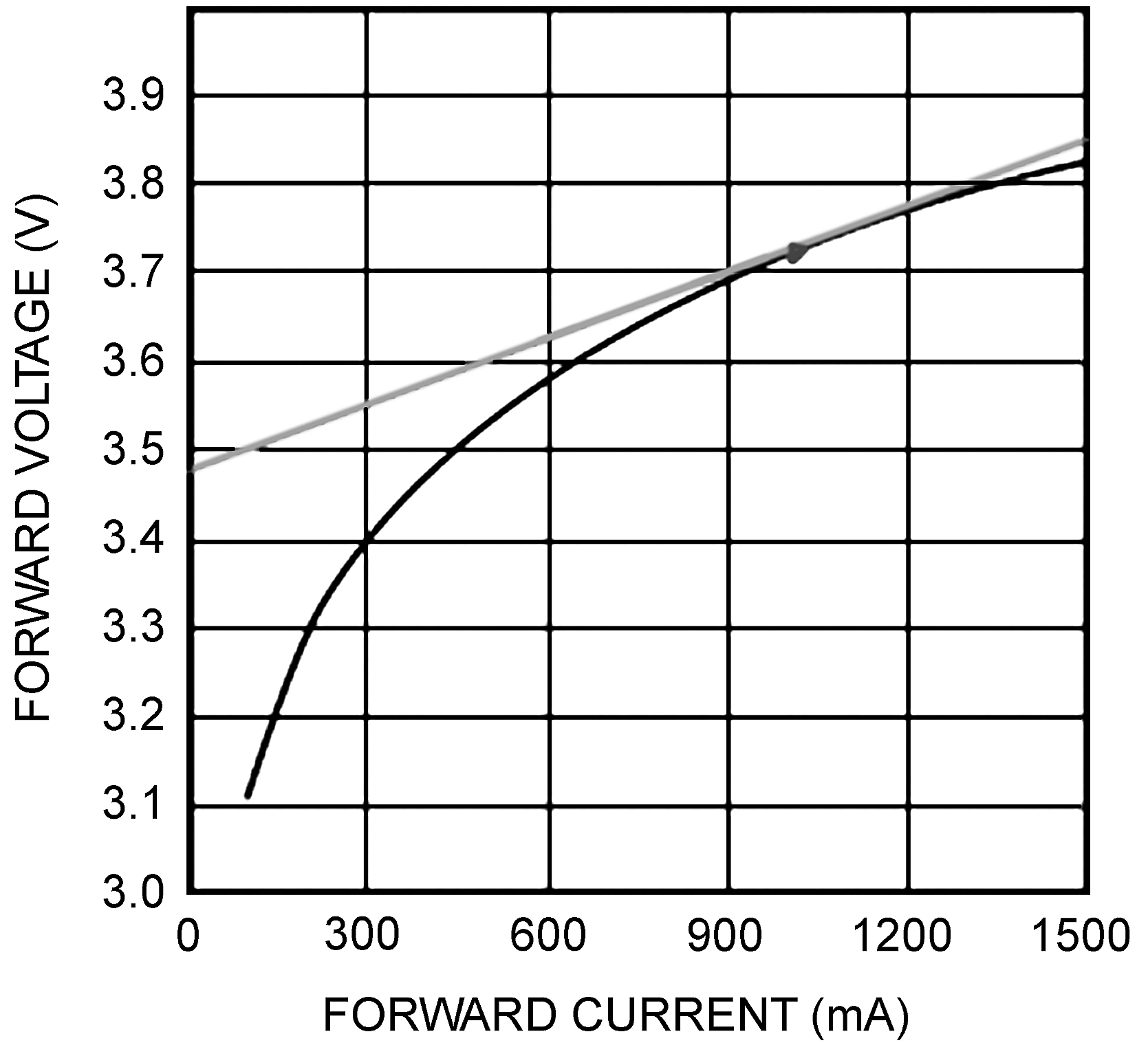 Figure 25. Dynamic Resistance
Obtaining rLED is accomplished by referring to the manufacturer's LED I-V characteristic. It can be calculated as the slope at the nominal operating point as shown in Figure 25. For any application with more than 2 series LEDs, RSNS can be neglected allowing rD to be approximated as the number of LEDs multiplied by rLED.
8.1.3 Output Capacitor
For boost and buck-boost regulators, the output capacitor (CO) provides energy to the load when the recirculating diode (D1) is reverse biased during the first switching subinterval. An output capacitor in a buck topology will simply reduce the LED current ripple (ΔiLED-PP) below the inductor current ripple (ΔiL-PP). In all cases, CO is sized to provide a desired ΔiLED-PP. As mentioned in the Inductor section, ΔiLED-PP is recommended by manufacturers to be less than 40% of the average LED current (ILED).
CO should be carefully chosen to account for derating due to temperature and operating voltage. It must also have the necessary RMS current rating. Ceramic capacitors are the best choice due to their high ripple current rating, long lifetime, and good temperature performance. An X7R dieletric rating is suggested.
8.1.4 Input Capacitors
The input capacitance (CIN) provides energy during the discontinuous portions of the switching period. For buck and buck-boost regulators, CIN provides energy during tON and during tOFF, the input voltage source charges up CIN with the average input current (IIN). For boost regulators, CIN only needs to provide the ripple current due to the direct connection to the inductor. CIN is selected given the maximum input voltage ripple (ΔvIN-PP) which can be tolerated. ΔvIN-PP is suggested to be less than 10% of the input voltage (VIN).
An input capacitance at least 100% greater than the calculated CIN value is recommended to account for derating due to temperature and operating voltage. When PWM dimming, even more capacitance can be helpful to minimize the large current draw from the input voltage source during the rising transition of the LED current waveform.
The chosen input capacitors must also have the necessary RMS current rating. Ceramic capacitors are again the best choice due to their high ripple current rating, long lifetime, and good temperature performance. An X7R dieletric rating is suggested.
For most applications, TI recommends bypassing the VIN pin with an 0.1-µF ceramic capacitor placed as close as possible to the pin. In situations where the bulk input capacitance may be far from the LM3429 device, a 10-Ω series resistor can be placed between the bulk input capacitance and the bypass capacitor, creating a 150 kHz filter to eliminate undesired high frequency noise coupling.
8.1.5 N-Channel MosFET (NFET)
The LM3429 requires an external NFET (Q1) as the main power MosFET for the switching regulator. Q1 is recommended to have a voltage rating at least 15% higher than the maximum transistor voltage to ensure safe operation during the ringing of the switch node. In practice, all switching regulators have some ringing at the switch node due to the diode parasitic capacitance and the lead inductance. The current rating is recommended to be at least 10% higher than the average transistor current. The power rating is then verified by calculating the power loss given the RMS transistor current and the NFET on-resistance (RDS-ON).
In general, the NFET should be chosen to minimize total gate charge (Qg) whenever switching frequencies are high and minimize RDS-ON otherwise. This will minimize the dominant power losses in the system. Frequently, higher current NFETs in larger packages are chosen for better thermal performance.
8.1.6 Re-Circulating Diode
A re-circulating diode (D1) is required to carry the inductor current during tOFF. The most efficient choice for D1 is a Schottky diode due to low forward voltage drop and near-zero reverse recovery time. Similar to Q1, D1 is recommended to have a voltage rating at least 15% higher than the maximum transistor voltage to ensure safe operation during the ringing of the switch node and a current rating at least 10% higher than the average diode current. The power rating is verified by calculating the power loss through the diode. This is accomplished by checking the typical diode forward voltage from the I-V curve on the product data sheet and multiplying by the average diode current. In general, higher current diodes have a lower forward voltage and come in better performing packages minimizing both power losses and temperature rise.
8.2 Typical Applications
8.2.1 Basic Topology Schematics
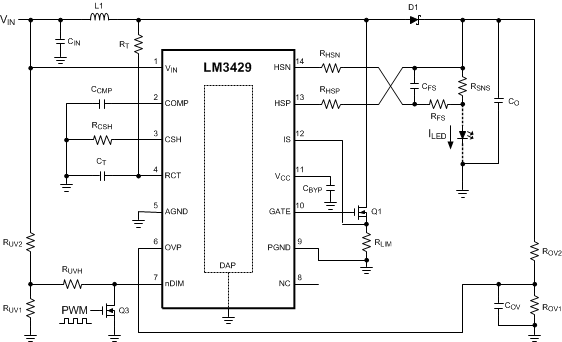 Figure 26. Boost Regulator (VIN < VO)
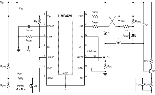 Figure 27. Buck Regulator (VIN > VO)
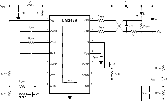 Figure 28. Buck-Boost Regulator
8.2.1.1 Design Requirements
Number of series LEDs: N
Single LED forward voltage: VLED
Single LED dynamic resistance: rLED
Nominal input voltage: VIN
Input voltage range: VIN-MAX, VIN-MIN
Switching frequency: fSW
Current sense voltage: VSNS
Average LED current: ILED
Inductor current ripple: ΔiL-PP
LED current ripple: ΔiLED-PP
Peak current limit: ILIM
Input voltage ripple: ΔvIN-PP
Output OVLO characteristics: VTURN-OFF, VHYSO
Input UVLO characteristics: VTURN-ON, VHYS
8.2.1.2 Detailed Design Procedure
8.2.1.2.1 Operating Point
Given the number of series LEDs (N), the forward voltage (VLED) and dynamic resistance (rLED) for a single LED, solve for the nominal output voltage (VO) and the nominal LED string dynamic resistance (rD):


Solve for the ideal nominal duty cycle (D):
Buck

Boost

Buck-boost

Using the same equations, find the minimum duty cycle (DMIN) using maximum input voltage (VIN-MAX) and the maximum duty cycle (DMAX) using the minimum input voltage (VIN-MIN). Also, remember that D' = 1 - D.
8.2.1.2.2 Switching Frequency
Set the switching frequency (fSW) by assuming a CT value of 1 nF and solving for RT:
Buck (Constant Ripple vs. VIN)

Buck (Constant Ripple vs. VO)

Boost and Buck-Boost

8.2.1.2.3 Average LED Current
For all topologies, set the average LED current (ILED) knowing the desired current sense voltage (VSNS) and solving for RSNS:

If the calculated RSNS is too far from a desired standard value, then VSNS must be adjusted to obtain a standard value.
Setup the suggested signal current of 100 µA by assuming RCSH = 12.4 kΩ and solving for RHSP:

If the calculated RHSP is too far from a desired standard value, then RCSH can be adjusted to obtain a standard value.
8.2.1.2.4 Inductor Ripple Current
Set the nominal inductor ripple current (ΔiL-PP) by solving for the appropriate inductor (L1):
Buck

Boost and Buck-Boost

To set the worst case inductor ripple current, use VIN-MAX and DMIN when solving for L1.
The minimum allowable inductor RMS current rating (IL-RMS) can be calculated as:
Buck

Boost and Buck-Boost

8.2.1.2.5 LED Ripple Current
Set the nominal LED ripple current (ΔiLED-PP), by solving for the output capacitance (CO):
Buck

Boost and Buck-Boost

To set the worst case LED ripple current, use DMAX when solving for CO.
The minimum allowable RMS output capacitor current rating (ICO-RMS) can be approximated:
Buck

Boost and Buck-boost

8.2.1.2.6 Peak Current Limit
Set the peak current limit (ILIM) by solving for the transistor path sense resistor (RLIM):

8.2.1.2.7 Loop Compensation
Using a simple first order peak current mode control model, neglecting any output capacitor ESR dynamics, the necessary loop compensation can be determined.
First, the uncompensated loop gain (TU) of the regulator can be approximated:
Buck

Boost and Buck-Boost

Where the pole (ωP1) is approximated:
Buck

Boost

Buck-Boost

And the RHP zero (ωZ1) is approximated:
Boost

Buck-Boost

And the uncompensated DC loop gain (TU0) is approximated:
Buck

Boost

Buck-Boost

For all topologies, the primary method of compensation is to place a low-frequency dominant pole (ωP2) which will ensure that there is ample phase margin at the crossover frequency. This is accomplished by placing a capacitor (CCMP) from the COMP pin to GND, which is calculated according to the lower value of the pole and the RHP zero of the system (shown as a minimizing function):


If analog dimming is used, CCMP should be approximately 4x larger to maintain stability as the LEDs are dimmed to zero.
A high frequency compensation pole (ωP3) can be used to attenuate switching noise and provide better gain margin. Assuming RFS = 10 Ω, CFS is calculated according to the higher value of the pole and the RHP zero of the system (shown as a maximizing function):


The total system loop gain (T) can then be written as:
Buck

Boost and Buck-boost

8.2.1.2.8 Input Capacitance
Set the nominal input voltage ripple (ΔvIN-PP) by solving for the required capacitance (CIN):
Buck

Boost

Buck-Boost

Use DMAX to set the worst case input voltage ripple, when solving for CIN in a buck-boost regulator and DMID = 0.5 when solving for CIN in a buck regulator.
The minimum allowable RMS input current rating (ICIN-RMS) can be approximated:
Buck

Boost

Buck-Boost

8.2.1.2.9 NFET
The NFET voltage rating should be at least 15% higher than the maximum NFET drain-to-source voltage (VT-MAX):
Buck

Boost

Buck-Boost

The current rating should be at least 10% higher than the maximum average NFET current (IT-MAX):
Buck

Boost and Buck-Boost

Approximate the nominal RMS transistor current (IT-RMS) :
Buck

Boost and Buck-Boost

Given an NFET with on-resistance (RDS-ON), solve for the nominal power dissipation (PT):

8.2.1.2.10 Diode
The Schottky diode voltage rating should be at least 15% higher than the maximum blocking voltage (VRD-MAX):
Buck

Boost

Buck-Boost

The current rating should be at least 10% higher than the maximum average diode current (ID-MAX):
Buck

Boost and Buck-Boost

Replace DMAX with D in the ID-MAX equation to solve for the average diode current (ID). Given a diode with forward voltage (VFD), solve for the nominal power dissipation (PD):

8.2.1.2.11 Output OVLO
For boost and buck-boost regulators, output OVLO is programmed with the turn-off threshold voltage (VTURN-OFF) and the desired hysteresis (VHYSO). To set VHYSO, solve for ROV2:

To set VTURN-OFF, solve for ROV1:
Boost

Buck-Boost

A small filter capacitor (COVP = 47 pF) should be added from the OVP pin to ground to reduce coupled switching noise.
8.2.1.2.12 Input UVLO
For all topologies, input UVLO is programmed with the turn-on threshold voltage (VTURN-ON) and the desired hysteresis (VHYS).
Method #1: If no PWM dimming is required, a two resistor network can be used. To set VHYS, solve for RUV2:

To set VTURN-ON, solve for RUV1:

Method #2: If PWM dimming is required, a three resistor network is suggested. To set VTURN-ON, assume RUV2 = 10 kΩ and solve for RUV1 as in Method #1. To set VHYS, solve for RUVH:

8.2.1.2.13 PWM Dimming Method
PWM dimming can be performed several ways:
Method #1: Connect the dimming MosFET (Q3) with the drain to the nDIM pin and the source to GND. Apply an external PWM signal to the gate of QDIM. A pull down resistor may be necessary to properly turn off Q3.
Method #2: Connect the anode of a Schottky diode to the nDIM pin. Apply an external inverted PWM signal to the cathode of the same diode.
8.2.1.2.14 Analog Dimming Method
Analog dimming can be performed several ways:
Method #1: Place a potentiometer in series with the RCSH resistor to dim the LED current from the nominal ILED to near zero.
Method #2: Connect a controlled current source as detailed in the Analog Dimming section to the CSH pin. Increasing the current sourced into the CSH node will decrease the LEDs from the nominal ILED to zero current.
8.2.2 Buck-Boost Application - 6 LEDs at 1 A
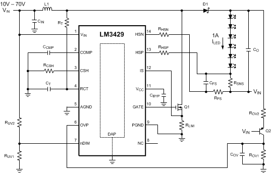 Figure 29. Buck-Boost Application - 6 LEDs at 1 A Schematic
8.2.2.1 Design Requirements
N = 6
VLED = 3.5 V
rLED = 325 mΩ
VIN = 24 V
VIN-MIN = 10 V
VIN-MAX = 70 V
fSW = 700 kHz
VSNS = 100 mV
ILED = 1A
ΔiL-PP = 500 mA
ΔiLED-PP = 50 mA
ΔvIN-PP = 100 mV
ILIM = 6A
VTURN-ON = 10 V
VHYS = 3 V
VTURN-OFF = 40 V
VHYSO = 10 V
8.2.2.2 Detailed Design Procedure
8.2.2.2.1 Operating Point
Solve for VO and rD:


Solve for D, D', DMAX, and DMIN:


8.2.2.2.2 Switching Frequency
Assume CT = 1 nF and solve for RT:

The closest standard resistor is actually 35.7 kΩ therefore the fSW is:

The chosen components from step 2 are:

8.2.2.2.3 Average LED Current
Solve for RSNS:

Assume RCSH = 12.4 kΩ and solve for RHSP:

The closest standard resistor for RSNS is actually 0.1Ω and for RHSP is actually 1 kΩ therefore ILED is:

The chosen components from step 3 are:

8.2.2.2.4 Inductor Ripple Current
Solve for L1:

The closest standard inductor is 33 µH therefore the actual ΔiL-PP is:

Determine minimum allowable RMS current rating:

The chosen component from step 4 is:

8.2.2.2.5 Output Capacitance
Solve for CO:

The closest standard capacitor is 6.8 µF therefore the actual ΔiLED-PP is:

Determine minimum allowable RMS current rating:

The chosen components from step 5 are:

8.2.2.2.6 Peak Current Limit
Solve for RLIM:

The closest standard resistor is 0.04 Ω therefore ILIM is:

The chosen component from step 6 is:

8.2.2.2.7 Loop Compensation
ωP1 is approximated:

ωZ1 is approximated:

TU0 is approximated:

To ensure stability, calculate ωP2:

Solve for CCMP:

To attenuate switching noise, calculate ωP3:

Assume RFS = 10 Ω and solve for CFS:

The chosen components from step 7 are:

8.2.2.2.8 Input Capacitance
Solve for the minimum CIN:

To minimize power supply interaction a 200% larger capacitance of approximately 14 µF is used, therefore the actual ΔvIN-PP is much lower. Because high voltage ceramic capacitor selection is limited, three 4.7 µF X7R capacitors are chosen.
Determine minimum allowable RMS current rating:

The chosen components from step 8 are:

8.2.2.2.9 NFET
Determine minimum Q1 voltage rating and current rating:


A 100-V NFET is chosen with a current rating of 32A due to the low RDS-ON = 50 mΩ. Determine IT-RMS and PT:


The chosen component from step 9 is:

8.2.2.2.10 Diode
Determine minimum D1 voltage rating and current rating:


A 100-V diode is chosen with a current rating of 12 A and VDF = 600 mV. Determine PD:

The chosen component from step 10 is:

8.2.2.2.11 Input UVLO
Solve for RUV2:

The closest standard resistor is 150 kΩ therefore VHYS is:

Solve for RUV1:

The closest standard resistor is 21 kΩ making VTURN-ON:

The chosen components from step 11 are:

8.2.2.2.12 Output OVLO
Solve for ROV2:

The closest standard resistor is 499 kΩ therefore VHYSO is:

Solve for ROV1:

The closest standard resistor is 15.8 kΩ making VTURN-OFF:

The chosen components from step 12 are:

Table 1. Design 1 Bill of Materials
| QTY | PART ID | PART VALUE | MANUFACTURER | PART NUMBER |
|---|---|---|---|---|
| 1 | LM3429 | Boost controller | TI | LM3429MH |
| 1 | CCMP | 0.22 µF X7R 10% 25 V | MURATA | GRM21BR71E224KA01L |
| 1 | CF | 2.2 µF X7R 10% 16 V | MURATA | GRM21BR71C225KA12L |
| 1 | CFS | 0.1 µF X7R 10% 25 V | MURATA | GRM21BR71E104KA01L |
| 3 | CIN | 4.7 µF X7R 10% 100 V | TDK | C5750X7R2A475K |
| 1 | CO | 6.8 µF X7R 10% 50 V | TDK | C4532X7R1H685K |
| 1 | COV | 47 pF COG/NPO 5% 50 V | AVX | 08055A470JAT2A |
| 1 | CT | 1000 pF COG/NPO 5% 50 V | MURATA | GRM2165C1H102JA01D |
| 1 | D1 | Schottky 100 V 12 A | VISHAY | 12CWQ10FNPBF |
| 1 | L1 | 33 µH 20% 6.3 A | COILCRAFT | MSS1278-333MLB |
| 1 | Q1 | NMOS 100 V 32 A | FAIRCHILD | FDD3682 |
| 1 | Q2 | PNP 150 V 600 m A | FAIRCHILD | MMBT5401 |
| 1 | RCSH | 12.4 kΩ 1% | VISHAY | CRCW080512K4FKEA |
| 1 | RFS | 10 Ω 1% | VISHAY | CRCW080510R0FKEA |
| 2 | RHSP, RHSN | 1 kΩ 1% | VISHAY | CRCW08051K00FKEA |
| 1 | RLIM | 0.04 Ω 1% 1W | VISHAY | WSL2512R0400FEA |
| 1 | ROV1 | 15.8 kΩ 1% | VISHAY | CRCW080515K8FKEA |
| 1 | ROV2 | 499 kΩ 1% | VISHAY | CRCW0805499KFKEA |
| 1 | RSNS | 0.1 Ω 1% 1W | VISHAY | WSL2512R1000FEA |
| 1 | RT | 35.7 kΩ 1% | VISHAY | CRCW080535K7FKEA |
| 1 | RUV1 | 21 kΩ 1% | VISHAY | CRCW080521K0FKEA |
| 1 | RUV2 | 150 kΩ 1% | VISHAY | CRCW0805150KFKEA |
8.2.2.3 Application Curve
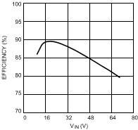 Figure 30. Buck-Boost Efficiency vs Input Voltage, VO= 6 LEDs
8.2.3 Boost PWM Dimming Application - 9 LEDs at 1 A
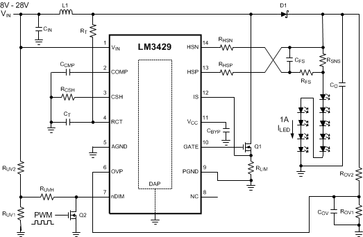 Figure 31. Boost PWM Dimming Application - 9 LEDs at 1 A Schematic
8.2.3.1 Detailed Design Procedure
Table 2. Design 2 Bill of Materials
| QTY | PART ID | PART VALUE | MANUFACTURER | PART NUMBER |
|---|---|---|---|---|
| 1 | LM3429 | Boost controller | TI | LM3429MH |
| 2 | CCMP, CFS | 0.1 µF X7R 10% 25 V | MURATA | GRM21BR71E104KA01L |
| 1 | CF | 2.2 µF X7R 10% 16 V | MURATA | GRM21BR71C225KA12L |
| 2, 1 | CIN, CO | 6.8 µF X7R 10% 50 V | TDK | C4532X7R1H685K |
| 1 | COV | 47 pF COG/NPO 5% 50 V | AVX | 08055A470JAT2A |
| 1 | CT | 1000 pF COG/NPO 5% 50 V | MURATA | GRM2165C1H102JA01D |
| 1 | D1 | Schottky 60 V 5 A | COMCHIP | CDBC560-G |
| 1 | L1 | 33 µH 20% 6.3 A | COILCRAFT | MSS1278-333MLB |
| 1 | Q1 | NMOS 60 V 8 A | VISHAY | SI4436DY |
| 1 | Q2 | NMOS 60 V 115 mA | ON SEMI | 2N7002ET1G |
| 2 | RCSH, ROV1 | 12.4 kΩ 1% | VISHAY | CRCW080512K4FKEA |
| 1 | RFS | 10 Ω 1% | VISHAY | CRCW080510R0FKEA |
| 2 | RHSP, RHSN | 1 kΩ 1% | VISHAY | CRCW08051K00FKEA |
| 1 | RLIM | 0.06 Ω 1% 1 W | VISHAY | WSL2512R0600FEA |
| 1 | ROV2 | 499 kΩ 1% | VISHAY | CRCW0805499KFKEA |
| 1 | RSNS | 0.1 Ω 1% 1 W | VISHAY | WSL2512R1000FEA |
| 1 | RT | 35.7 kΩ 1% | VISHAY | CRCW080535K7FKEA |
| 1 | RUV1 | 1.82 kΩ 1% | VISHAY | CRCW08051K82FKEA |
| 1 | RUV2 | 10 kΩ 1% | VISHAY | CRCW080510KFKEA |
| 1 | RUVH | 17.8 kΩ 1% | VISHAY | CRCW080517K8FKEA |
8.2.4 Buck-Boost Analog Dimming Application - 4 LEDs at 2A
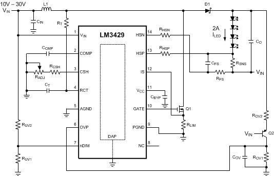 Figure 32. Buck-Boost Analog Dimming Application - 4 LEDs at 2 A Schematic
8.2.4.1 Detailed Design Procedure
Table 3. Bill of Materials
| QTY | PART ID | PART VALUE | MANUFACTURER | PART NUMBER |
|---|---|---|---|---|
| 1 | LM3429 | Boost controller | TI | LM3429MH |
| 1 | CCMP | 1 µF X7R 10% 10 V | MURATA | GRM21BR71A105KA01L |
| 1 | CF | 2.2 µF X7R 10% 16 V | MURATA | GRM21BR71C225KA12L |
| 1 | CFS | 0.1 µF X7R 10% 50 V | MURATA | GRM21BR71E104KA01L |
| 2, 1 | CIN, CO | 6.8 µF X7R 10% 50 V | TDK | C4532X7R1H685K |
| 1 | COV | 47 pF COG/NPO 5% 50 V | AVX | 08055A470JAT2A |
| 1 | CT | 1000 pF COG/NPO 5% 50 V | MURATA | GRM2165C1H102JA01D |
| 1 | D1 | Schottky 60 V 5 A | VISHAY | CDBC560-G |
| 1 | L1 | 22 µH 20% 7.2 A | COILCRAFT | MSS1278-223MLB |
| 1 | Q1 | NMOS 60 V 8 A | VISHAY | SI4436DY |
| 1 | Q2 | PNP 150 V 600 mA | FAIRCHILD | MMBT5401 |
| 1 | RADJ | 1-MΩ potentiometer | BOURNS | 3352P-1-105 |
| 1 | RCSH | 12.4 kΩ 1% | VISHAY | CRCW080512K4FKEA |
| 1 | RFS | 10 Ω 1% | VISHAY | CRCW080510R0FKEA |
| 2 | RHSP, RHSN | 1 kΩ 1% | VISHAY | CRCW08051K00FKEA |
| 1 | RLIM | 0.04 Ω 1% 1 W | VISHAY | WSL2512R0400FEA |
| 1 | ROV1 | 18.2 kΩ 1% | VISHAY | CRCW080518K2FKEA |
| 1 | ROV2 | 499 kΩ 1% | VISHAY | CRCW0805499KFKEA |
| 1 | RSNS | 0.05 Ω 1% 1 W | VISHAY | WSL2512R0500FEA |
| 1 | RT | 41.2 kΩ 1% | VISHAY | CRCW080541K2FKEA |
| 1 | RUV1 | 21 kΩ 1% | VISHAY | CRCW080521K0FKEA |
| 1 | RUV2 | 150 kΩ 1% | VISHAY | CRCW0805150KFKEA |
8.2.5 Boost Analog Dimming Application - 12 LEDs at 700 mA
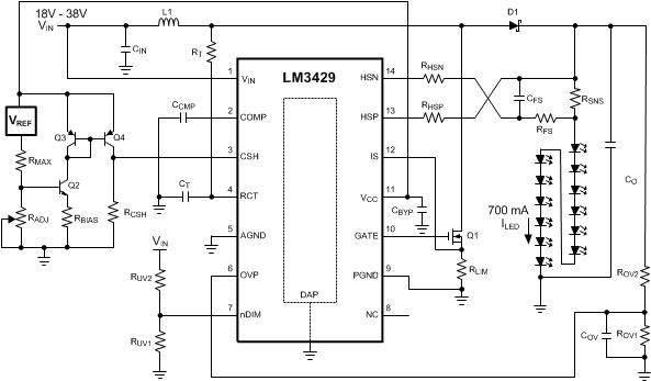 Figure 33. Boost Analog Dimming Application - 12 LEDs at 700 mA Schematic
8.2.5.1 Detailed Design Procedure
Table 4. Bill of Materials
| QTY | PART ID | PART VALUE | MANUFACTURER | PART NUMBER |
|---|---|---|---|---|
| 1 | LM3429 | Boost controller | TI | LM3429MH |
| 1 | CCMP | 1 µF X7R 10% 10 V | MURATA | GRM21BR71A105KA01L |
| 1 | CF | 2.2 µF X7R 10% 16 V | MURATA | GRM21BR71C225KA12L |
| 1 | CFS | 0.1 µF X7R 10% 50 V | MURATA | GRM21BR71E104KA01L |
| 2, 1 | CIN, CO | 6.8 µF X7R 10% 50 V | TDK | C4532X7R1H685K |
| 1 | COV | 47 pF COG/NPO 5% 50 V | AVX | 08055A470JAT2A |
| 1 | CT | 1000 pF COG/NPO 5% 50 V | MURATA | GRM2165C1H102JA01D |
| 1 | D1 | Schottky 100 V 12 A | VISHAY | 12CWQ10FNPBF |
| 1 | L1 | 47 µH 20% 5.3 A | COILCRAFT | MSS1278-473MLB |
| 1 | Q1 | NMOS 100 V 32 A | FAIRCHILD | FDD3682 |
| 1 | Q2 | NPN 40 V 200 mA | FAIRCHILD | MMBT3904 |
| 1 | Q3, Q4 (dual pack) | Dual PNP 40 V 200 mA | FAIRCHILD | FFB3906 |
| 1 | RADJ | 100 kΩ potentiometer | BOURNS | 3352P-1-104 |
| 1 | RBIAS | 40.2 kΩ 1% | VISHAY | CRCW080540K2FKEA |
| 1 | RCSH, ROV1, RUV1 | 12.4 kΩ 1% | VISHAY | CRCW080512K4FKEA |
| 1 | RFS | 10 Ω 1% | VISHAY | CRCW080510R0FKEA |
| 2 | RHSP, RHSN | 1.05 kΩ 1% | VISHAY | CRCW08051K05FKEA |
| 1 | RLIM | 0.06 Ω 1% 1 W | VISHAY | WSL2512R0600FEA |
| 1 | RMAX | 4.99 kΩ 1% | VISHAY | CRCW08054K99FKEA |
| 1 | ROV2 | 499 kΩ 1% | VISHAY | CRCW0805499KFKEA |
| 1 | RSNS | 0.15 Ω 1% 1 W | VISHAY | WSL2512R1500FEA |
| 1 | RT | 35.7 kΩ 1% | VISHAY | CRCW080535K7FKEA |
| 1 | RUV2 | 100 kΩ 1% | VISHAY | CRCW0805100KFKEA |
| 1 | VREF | 5 V precision reference | TI | LM4040 |
8.2.6 Buck-Boost PWM Dimming Application - 6 LEDs at 500 mA
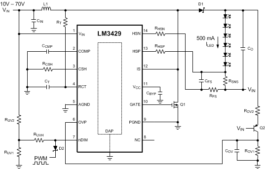 Figure 34. Buck-Boost PWM Dimming Application - 6 LEDs at 500 mA
8.2.6.1 Detailed Design Procedure
Table 5. Bill of Materials
| QTY | PART ID | PART VALUE | MANUFACTURER | PART NUMBER |
|---|---|---|---|---|
| 1 | LM3429 | Boost controller | TI | LM3429MH |
| 1 | CCMP | 0.68 µF X7R 10% 25 V | MURATA | GRM21BR71E684KA88L |
| 1 | CF | 2.2 µF X7R 10% 16 V | MURATA | GRM21BR71C225KA12L |
| 1 | CFS | 0.1 µF X7R 10% 25 V | MURATA | GRM21BR71E104KA01L |
| 3 | CIN | 4.7 µF X7R 10% 100 V | TDK | C5750X7R2A475K |
| 1 | CO | 6.8 µF X7R 10% 50 V | TDK | C4532X7R1H685K |
| 1 | COV | 47 pF COG/NPO 5% 50 V | AVX | 08055A470JAT2A |
| 1 | CT | 1000 pF COG/NPO 5% 50 V | MURATA | GRM2165C1H102JA01D |
| 1 | D1 | Schottky 100 V 12 A | VISHAY | 12CWQ10FNPBF |
| 1 | D2 | Schottky 30 V 500 mA | ON SEMI | BAT54T1G |
| 1 | L1 | 68 µH 20% 4.3 A | COILCRAFT | MSS1278-683MLB |
| 1 | Q1 | NMOS 100 V 32 A | VISHAY | FDD3682 |
| 1 | Q2 | PNP 150 V 600 mA | FAIRCHILD | MMBT5401 |
| 1 | RCSH | 12.4 kΩ 1% | VISHAY | CRCW080512K4FKEA |
| 1 | RFS | 10 Ω 1% | VISHAY | CRCW080510R0FKEA |
| 2 | RHSP, RHSN | 1 kΩ 1% | VISHAY | CRCW08051K00FKEA |
| 1 | ROV1 | 15.8 kΩ 1% | VISHAY | CRCW080515K8FKEA |
| 1 | ROV2 | 499 kΩ 1% | VISHAY | CRCW0805499KFKEA |
| 1 | RSNS | 0.2 Ω 1% 1 W | VISHAY | WSL2512R2000FEA |
| 1 | RT | 35.7 kΩ 1% | VISHAY | CRCW080535K7FKEA |
| 1 | RUV1 | 1.43 kΩ 1% | VISHAY | CRCW08051K43FKEA |
| 1 | RUV2 | 10 kΩ 1% | VISHAY | CRCW080510K0FKEA |
| 1 | RUVH | 17.4 kΩ 1% | VISHAY | CRCW080517K4FKEA |
8.2.7 Buck Application - 3 LEDS at 1.25 A
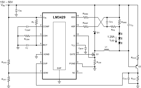 Figure 35. Buck Application - 3 LEDS at 1.25 A Schematic
8.2.7.1 Detailed Design Procedure
Table 6. Bill of Materials
| QTY | PART ID | PART VALUE | MANUFACTURER | PART NUMBER |
|---|---|---|---|---|
| 1 | LM3429 | Boost controller | TI | LM3429MH |
| 1 | CCMP | 0.015 µF X7R 10% 50 V | MURATA | GRM21BR71H153KA01L |
| 1 | CF | 2.2 µF X7R 10% 16 V | MURATA | GRM21BR71C225KA12L |
| 1 | CFS | 0.01 µF X7R 10% 50 V | MURATA | GRM21BR71H103KA01L |
| 2 | CIN | 6.8 µF X7R 10% 50 V | TDK | C4532X7R1H685K |
| 1 | CO | 1 µF X7R 10% 50 V | TDK | C4532X7R1H105K |
| 1 | COV | 47 pF COG/NPO 5% 50 V | AVX | 08055A470JAT2A |
| 1 | CT | 1000 pF COG/NPO 5% 50 V | MURATA | GRM2165C1H102JA01D |
| 1 | D1 | Schottky 60V 5 A | COMCHIP | CDBC560-G |
| 1 | L1 | 22 µH 20% 7.3 A | COILCRAFT | MSS1278-223MLB |
| 1 | Q1 | NMOS 60 V 8 A | VISHAY | SI4436DY |
| 1 | Q2 | PNP 150 V 600 mA | FAIRCHILD | MMBT5401 |
| 1 | RCSH | 12.4 kΩ 1% | VISHAY | CRCW080512K4FKEA |
| 1 | RT | 49.9 kΩ 1% | VISHAY | CRCW080549K9FKEA |
| 1 | RFS | 10 Ω 1% | VISHAY | CRCW080510R0FKEA |
| 2 | RHSP, RHSN | 1 kΩ 1% | VISHAY | CRCW08051K00FKEA |
| 1 | RLIM | 0.04 Ω 1% 1 W | VISHAY | WSL2512R0400FEA |
| 1 | ROV1 | 21.5 kΩ 1% | VISHAY | CRCW080521K5FKEA |
| 1 | ROV2 | 499 kΩ 1% | VISHAY | CRCW0805499KFKEA |
| 1 | RSNS | 0.08 Ω 1% 1 W | VISHAY | WSL2512R0800FEA |
| 1 | RUV1 | 11.5 kΩ 1% | VISHAY | CRCW080511K5FKEA |
| 1 | RUV2 | 100 kΩ 1% | VISHAY | CRCW0805100KFKEA |
8.2.8 Buck-Boost Thermal Foldback Application - 8 LEDs at 2.5 A
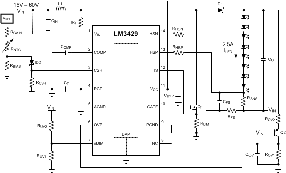 Figure 36. Buck-Boost Thermal Foldback Application - 8 LEDs at 2.5 A Schematic
8.2.8.1 Detailed Design Procedure
Table 7. Bill of Materials
| QTY | PART ID | PART VALUE | MANUFACTURER | PART NUMBER |
|---|---|---|---|---|
| 1 | LM3429 | Boost controller | TI | LM3429MH |
| 1 | CCMP | 0.1 µF X7R 10% 25 V | MURATA | GRM21BR71E104KA01L |
| 1 | CF | 2.2 µF X7R 10% 16 V | MURATA | GRM21BR71C225KA12L |
| 1 | CFS | 0.1 µF X7R 10% 25 V | MURATA | GRM21BR71E104KA01L |
| 3 | CIN | 4.7 µF X7R 10% 100 V | TDK | C5750X7R2A475K |
| 1 | CO | 6.8 µF X7R 10% 50 V | TDK | C4532X7R1H685K |
| 1 | COV | 47 pF COG/NPO 5% 50 V | AVX | 08055A470JAT2A |
| 1 | CT | 1000 pF COG/NPO 5% 50 V | MURATA | GRM2165C1H102JA01D |
| 1 | D1 | Schottky 100 V 12 A | VISHAY | 12CWQ10FNPBF |
| 1 | L1 | 22 µH 20% 7.2 A | COILCRAFT | MSS1278-223MLB |
| 1 | Q1 | NMOS 100 V 32 A | FAIRCHILD | FDD3682 |
| 1 | Q2 | PNP 150 V 600 mA | FAIRCHILD | MMBT5401 |
| 2 | RCSH, ROV1 | 12.4 kΩ 1% | VISHAY | CRCW080512K4FKEA |
| 1 | RFS | 10 Ω 1% | VISHAY | CRCW080510R0FKEA |
| 2 | RHSP, RHSN | 1 kΩ 1% | VISHAY | CRCW08051K00FKEA |
| 2 | RLIM, RSNS | 0.04 Ω 1% 1 W | VISHAY | WSL2512R0400FEA |
| 1 | ROV2 | 499 kΩ 1% | VISHAY | CRCW0805499KFKEA |
| 1 | RT | 49.9 kΩ 1% | VISHAY | CRCW080549K9FKEA |
| 1 | RUV1 | 13.7 kΩ 1% | VISHAY | CRCW080513K7FKEA |
| 1 | RUV2 | 150 kΩ 1% | VISHAY | CRCW0805150KFKEA |
8.2.9 SEPIC Application - 5 LEDs at 750 mA
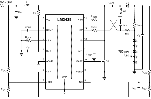 Figure 37. 5 LEDs at 750 mA