ZHCSDP4B May 2015 – February 2017 LM2776
PRODUCTION DATA.
7 Detailed Description
7.1 Overview
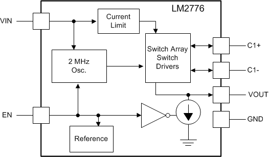
The LM2776 CMOS charge-pump voltage converter inverts a positive voltage in the range of 2.7 V to 5.5 V to the corresponding negative voltage of −2.7 V to −5.5 V. The LM2776 uses three low-cost capacitors to provide up to 200 mA of output current.
7.2 Functional Block Diagram

7.3 Feature Description
7.3.1 Input Current Limit
The LM2776 contains current limit circuitry that protects the device in the event of excessive input current and/or output shorts to ground. The input current is limited to 400 mA (typical at VIN = 5.5 V) when the output is shorted directly to ground. When the LM2776 is current limiting, power dissipation in the device is likely to be quite high. In this event, thermal cycling is expected.
7.3.2 PFM Operation
To minimize quiescent current during light load operation, the LM2776 allows PFM or pulse-skipping operation. By allowing the charge pump to switch less when the output current is less than 40 mA, the quiescent current drawn from the power source is minimized. The frequency of pulsed operation is not limited and can drop into the sub-1-kHz range when unloaded. As the load increases, the frequency of pulsing increases until it transitions to constant frequency. The fundamental switching frequency of the LM2776 is 2 MHz.
7.3.3 Output Discharge
In shutdown, the LM2776 actively pulls down on the output of the device until the output voltage reaches GND. In this mode, the current drawn from the output is approximately 1.85 mA.
7.3.4 Thermal Shutdown
The LM2776 implements a thermal shutdown mechanism to protect the device from damage due to overheating. When the junction temperature rises to 150°C (typical), the part switches into shutdown mode. The LM2776 releases thermal shutdown when the junction temperature of the part is reduced to 130°C (typical).
Thermal shutdown is most often triggered by self-heating, which occurs when there is excessive power dissipation in the device and/or insufficient thermal dissipation. LM2776 power dissipation increases with increased output current and input voltage. When self-heating brings on thermal shutdown, thermal cycling is the typical result. Thermal cycling is the repeating process where the part self-heats, enters thermal shutdown (where internal power dissipation is practically zero), cools, turns on, and then heats up again to the thermal shutdown threshold. Thermal cycling is recognized by a pulsing output voltage and can be stopped be reducing the internal power dissipation (reduce input voltage and/or output current) or the ambient temperature. If thermal cycling occurs under desired operating conditions, thermal dissipation performance must be improved to accommodate the power dissipation of the LM2776.
7.3.5 Undervoltage Lockout
The LM2776 has an internal comparator that monitors the voltage at VIN and forces the device into shutdown if the input voltage drops to 2.4 V. If the input voltage rises above 2.6 V, the LM2776 resumes normal operation.
7.4 Device Functional Modes
7.4.1 Shutdown Mode
An enable pin (EN) pin is available to disable the device and place the LM2776 into shutdown mode reducing the quiescent current to 1 µA. In shutdown, the output of the LM2776 is pulled to ground by an internal pullup current source (approx 1.85 mA).
7.4.2 Enable Mode
Applying a voltage greater than 1.2 V to the EN pin places the device into enable mode. When unloaded, the input current during operation is 120 µA. As the load current increases, so does the quiescent current. When enabled, the output voltage is equal to the inverse of the input voltage minus the voltage drop across the charge pump.