ZHCSDP4B May 2015 – February 2017 LM2776
PRODUCTION DATA.
6 Specifications
6.1 Absolute Maximum Ratings
over operating free-air temperature range (unless otherwise noted)(1)(2)| MIN | MAX | UNIT | ||
|---|---|---|---|---|
| Supply voltage (VIN to GND, or GND to VOUT) | 6 | V | ||
| EN | (GND − 0.3) | (VIN + 0.3) | V | |
| VOUT continuous output current | 250 | mA | ||
| Operating junction temperature, TJMax(3) | 125 | °C | ||
| Storage temperature, Tstg | –65 | 150 | °C | |
(1) Stresses beyond those listed under Absolute Maximum Ratings may cause permanent damage to the device. These are stress ratings only, which do not imply functional operation of the device at these or any other conditions beyond those indicated under Recommended Operating Conditions. Exposure to absolute-maximum-rated conditions for extended periods may affect device reliability.
(2) If Military/Aerospace specified devices are required, contact the Texas Instruments Sales Office/Distributors for availability and specifications.
(3) The maximum allowable power dissipation is calculated by using PDMax = (TJMax − TA) / RθJA, where TJMax is the maximum junction temperature, TA is the ambient temperature, and RθJA is the junction-to-ambient thermal resistance of the specified package.
6.2 ESD Ratings
| VALUE | UNIT | |||
|---|---|---|---|---|
| V(ESD) | Electrostatic discharge | Human-body model (HBM), per ANSI/ESDA/JEDEC JS-001(1) | ±1000 | V |
| Charged-device model (CDM), per JEDEC specification JESD22-C101(2) | ±250 | V | ||
(1) JEDEC document JEP155 states that 500-V HBM allows safe manufacturing with a standard ESD control process.
(2) JEDEC document JEP157 states that 250-V CDM allows safe manufacturing with a standard ESD control process.
6.3 Recommended Operating Conditions
over operating free-air temperature range (unless otherwise noted)| MIN | NOM | MAX | UNIT | ||
|---|---|---|---|---|---|
| Junction temperature | –40 | 125 | °C | ||
| Ambient temperature | –40 | 85 | °C | ||
| Input voltage | 2.7 | 5.5 | V | ||
| Output current | 0 | 200 | mA | ||
6.4 Thermal Information
| THERMAL METRIC(1) | LM2776 | UNIT | |
|---|---|---|---|
| DBV (SOT) | |||
| 6 PINS | |||
| RθJA | Junction-to-ambient thermal resistance | 187 | °C/W |
| RθJC(top) | Junction-to-case (top) thermal resistance | 158.2 | °C/W |
| RθJB | Junction-to-board thermal resistance | 33.3 | °C/W |
| ψJT | Junction-to-top characterization parameter | 37.8 | °C/W |
| ψJB | Junction-to-board characterization parameter | 32.8 | °C/W |
(1) For more information about traditional and new thermal metrics, see the Semiconductor and IC Package Thermal Metrics application report, SPRA953.
6.5 Electrical Characteristics
Typical limits tested at TA = 25°C. Minimum and maximum limits apply over the full operating ambient temperature range (−40°C ≤ TA ≤ +85°C). VIN = 3.6 V, CIN = COUT = 2.2 µF, C1 = 1 µF| PARAMETER | TEST CONDITIONS | MIN | TYP | MAX | UNIT | |
|---|---|---|---|---|---|---|
| IQ | Supply current | EN = 1. No load | 100 | 200 | µA | |
| ISD | Shutdown supply current | EN = 0 | 0.1 | 1 | µA | |
| VEN | Enable pin input threshold voltage | Normal operation | 1.2 | V | ||
| Shutdown mode | 0.4 | |||||
| ROUT | Output resistance | 2.5 | Ω | |||
| ICL | Output current limit | 400 | mA | |||
| UVLO | Undervoltage lockout | VIN Falling | 2.4 | V | ||
| VIN Rising | 2.6 | |||||
6.6 Switching Characteristics
over operating free-air temperature range (unless otherwise noted)| PARAMETER | TEST CONDITIONS | MIN | TYP | MAX | UNIT | |
|---|---|---|---|---|---|---|
| ƒSW | Switching frequency | 1.7 | 2 | 2.3 | MHz | |
6.7 Typical Characteristics
(典型应用 circuit, VIN = 3.6 V unless otherwise specified.)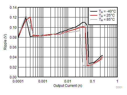
| VIN = 5.5 V |
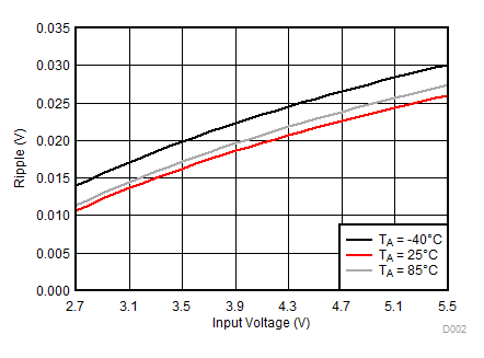
| IOUT = 100 mA |
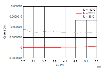
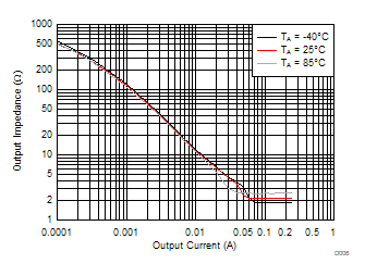
| VIN = 5.5 V |
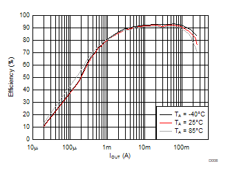
| VIN = 3.6 V |
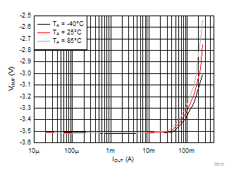
| VIN = 3.6 V |
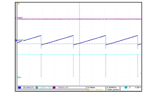
| IOUT = 0 mA | VIN = 5.5 V |
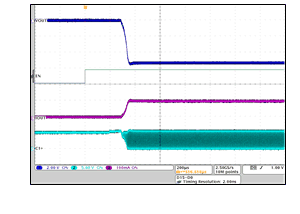
| EN = 1 | VIN = 5.5 V | IOUT = 100 mA |
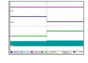
| IOUT = 75 mA |
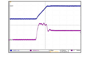
| VIN = 5.5 V |
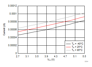
| No load |
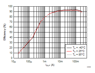
| VIN = 5.5 V |
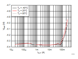
| VIN = 5.5 V |
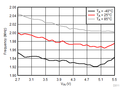
| IOUT = 150 mA |
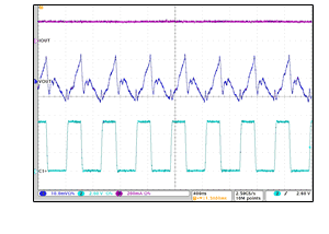
| IOUT = 200 mA | VIN = 5.5 V |
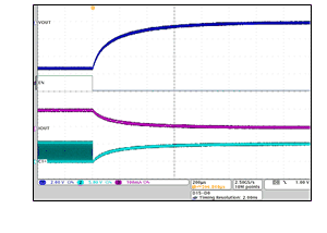
| EN = 0 | VIN = 5.5 V | IOUT = 100 mA |
| VIN = 5.5 V |