SNVS316H September 2004 – December 2014 LM2736
PRODUCTION DATA.
- 1 Features
- 2 Applications
- 3 Description
- 4 Revision History
- 5 Pin Configuration and Functions
- 6 Specifications
- 7 Detailed Description
-
8 Application and Implementation
- 8.1 Application Information
- 8.2
Typical Applications
- 8.2.1 LM2736X (1.6 MHz) VBOOST Derived from VIN 5 V to 1.5 V / 750 mA
- 8.2.2 LM2736X (1.6 MHz) VBOOST Derived from VOUT 12 V to 3.3 V / 750 mA
- 8.2.3 LM2736X (1.6 MHz) VBOOST Derived from VSHUNT 18 V to 1.5 V / 750 mA
- 8.2.4 LM2736X (1.6 MHz) VBOOST Derived from Series Zener Diode (VIN) 15 V to 1.5 V / 750 mA
- 8.2.5 LM2736X (1.6 MHz) VBOOST Derived from Series Zener Diode (VOUT) 15 V to 9 V / 750 mA
- 8.2.6 LM2736Y (550 kHz) VBOOST Derived from VIN 5 V to 1.5 V / 750 mA
- 8.2.7 LM2736Y (550 kHz) VBOOST Derived from VOUT 12 V to 3.3 V / 750 mA
- 8.2.8 LM2736Y (550 kHz) VBOOST Derived from VSHUNT 18 V to 1.5 V / 750 mA
- 8.2.9 LM2736Y (550 kHz) VBOOST Derived from Series Zener Diode (VIN) 15 V to 1.5 V / 750 mA
- 8.2.10 LM2736Y (550 kHz) VBOOST Derived from Series Zener Diode (VOUT) 15 V to 9 V / 750 mA
- 9 Power Supply Recommendations
- 10Layout
- 11Device and Documentation Support
- 12Mechanical, Packaging, and Orderable Information
6 Specifications
6.1 Absolute Maximum Ratings
over operating free-air temperature range (unless otherwise noted)(1)| MIN | MAX | UNIT | ||
|---|---|---|---|---|
| VIN | -0.5 | 22 | V | |
| SW Voltage | -0.5 | 22 | V | |
| Boost Voltage | -0.5 | 28 | V | |
| Boost to SW Voltage | -0.5 | 8 | V | |
| FB Voltage | -0.5 | 3 | V | |
| EN Voltage | -0.5 | VIN + 0.3 | V | |
| Junction Temperature | 150 | °C | ||
| Soldering Information | Infrared/Convection Reflow (15sec) | 220 | °C | |
| Wave Soldering Lead temperature (10sec) | 260 | °C | ||
| Tstg | Storage temperature | -65 | 150 | °C |
6.2 ESD Ratings
| VALUE | UNIT | ||||
|---|---|---|---|---|---|
| V(ESD) | Electrostatic discharge | Human body model (HBM), per ANSI/ESDA/JEDEC JS-001, all pins(1) |
±2000 | V | |
(1) JEDEC document JEP155 states that 500-V HBM allows safe manufacturing with a standard ESD control process.
6.3 Recommended Operating Conditions
over operating free-air temperature range (unless otherwise noted)| MIN | NOM | MAX | UNIT | ||
|---|---|---|---|---|---|
| VIN | 3 | 18 | V | ||
| SW Voltage | -0.5 | 18 | V | ||
| Boost Voltage | -0.5 | 23 | V | ||
| Boost to SW Voltage | 1.6 | 5.5 | V | ||
| Junction Temperature Range | −40 | 125 | °C | ||
6.4 Thermal Information
| THERMAL METRIC(1) | LM2736 | UNIT | |
|---|---|---|---|
| DDC | |||
| 6 PINS | |||
| RθJA(2) | Junction-to-ambient thermal resistance | 158.1 | °C/W |
| RθJC(top) | Junction-to-case (top) thermal resistance | 46.5 | |
| RθJB | Junction-to-board thermal resistance | 29.5 | |
| ψJT | Junction-to-top characterization parameter | 0.8 | |
| ψJB | Junction-to-board characterization parameter | 29.2 | |
| RθJC(bot) | Junction-to-case (bottom) thermal resistance | n/a | |
(1) For more information about traditional and new thermal metrics, see the IC Package Thermal Metrics application report, SPRA953.
6.5 Electrical Characteristics
Specifications with standard typeface are for TJ = 25°C unless otherwise specified. Datasheet min/max specification limits are ensured by design, test, or statistical analysis.| PARAMETER | TEST CONDITIONS | TJ = 25°C | TJ = -40°C to 125°C | UNIT | ||||||
|---|---|---|---|---|---|---|---|---|---|---|
| MIN(3) | TYP(4) | MAX(3) | MIN | TYP | MAX | |||||
| VFB | Feedback Voltage | 1.250 | 1.225 | 1.275 | V | |||||
| ΔVFB/ΔVIN | Feedback Voltage Line Regulation | VIN = 3V to 18V | 0.01 | % / V | ||||||
| IFB | Feedback Input Bias Current | Sink/Source | 10 | 250 | nA | |||||
| UVLO | Undervoltage Lockout | VIN Rising | 2.74 | 2.90 | V | |||||
| Undervoltage Lockout | VIN Falling | 2.3 | 2.0 | |||||||
| UVLO Hysteresis | 0.44 | 0.30 | 0.62 | |||||||
| FSW | Switching Frequency | LM2736X | 1.6 | 1.2 | 1.9 | MHz | ||||
| LM2736Y | 0.55 | 0.40 | 0.66 | |||||||
| DMAX | Maximum Duty Cycle | LM2736X | 92% | 85% | ||||||
| LM2736Y | 96% | 90% | ||||||||
| DMIN | Minimum Duty Cycle | LM2736X | 2% | |||||||
| LM2736Y | 1% | |||||||||
| RDS(ON) | Switch ON Resistance | VBOOST - VSW = 3V | 350 | 650 | mΩ | |||||
| ICL | Switch Current Limit | VBOOST - VSW = 3V | 1.5 | 1.0 | 2.3 | A | ||||
| IQ | Quiescent Current | Switching | 1.5 | 2.5 | mA | |||||
| Quiescent Current (shutdown) | VEN = 0V | 30 | nA | |||||||
| IBOOST | Boost Pin Current | LM2736X (50% Duty Cycle) | 2.2 | 3.3 | mA | |||||
| LM2736Y (50% Duty Cycle) | 0.9 | 1.6 | ||||||||
| VEN_TH | Shutdown Threshold Voltage | VEN Falling | 0.4 | V | ||||||
| Enable Threshold Voltage | VEN Rising | 1.8 | ||||||||
| IEN | Enable Pin Current | Sink/Source | 10 | nA | ||||||
| ISW | Switch Leakage | 40 | nA | |||||||
(1) If Military/Aerospace specified devices are required, please contact the Texas Instruments Sales Office/ Distributors for availability and specifications.
(2) Thermal shutdown will occur if the junction temperature exceeds 165°C. The maximum power dissipation is a function of TJ(MAX) , θJA and TA . The maximum allowable power dissipation at any ambient temperature is PD = (TJ(MAX) – TA)/θJA . All numbers apply for packages soldered directly onto a 3” x 3” PC board with 2oz. copper on 4 layers in still air. For a 2 layer board using 1 oz. copper in still air, θJA = 204°C/W.
(3) Specified to Texas Instruments' Average Outgoing Quality Level (AOQL).
(4) Typicals represent the most likely parametric norm.
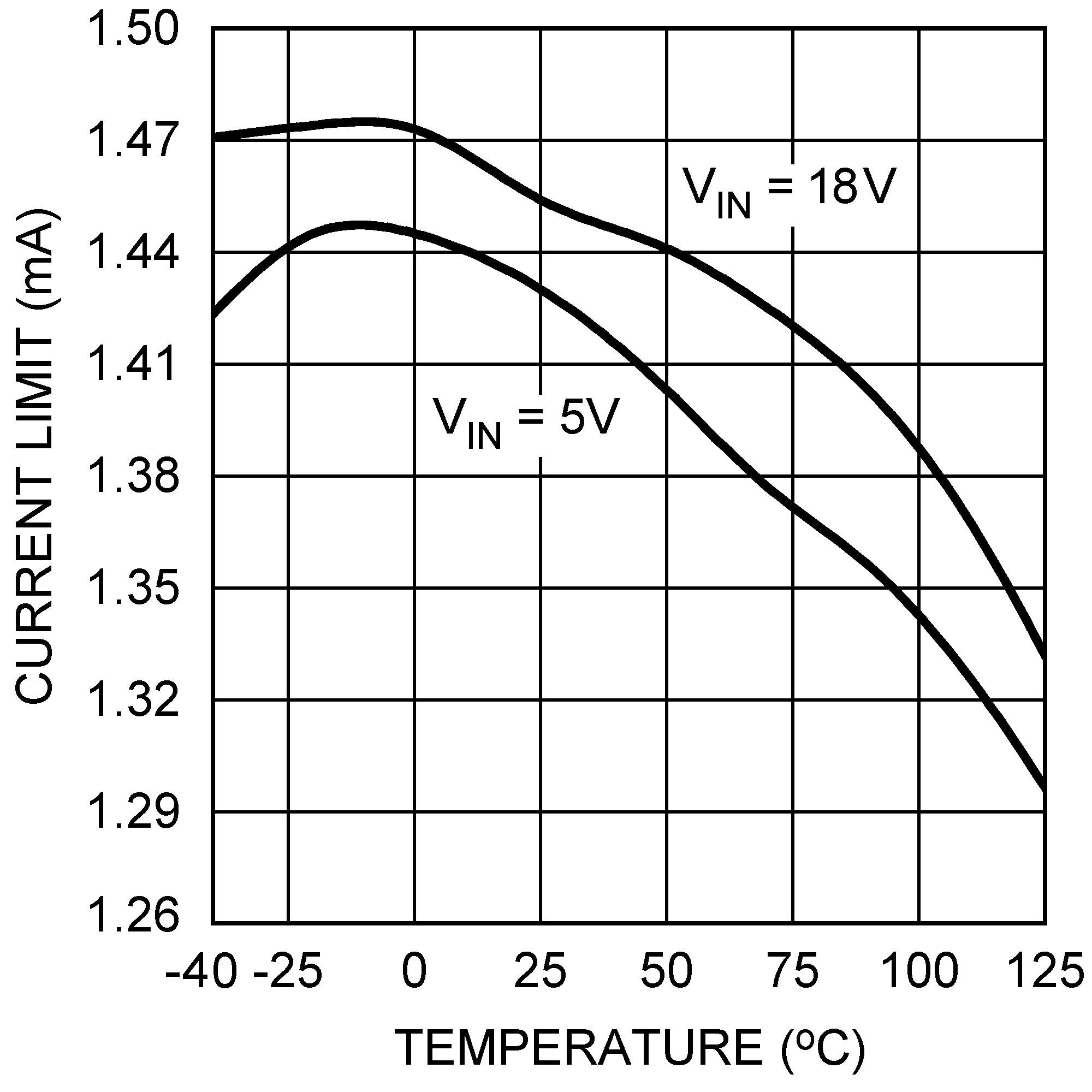
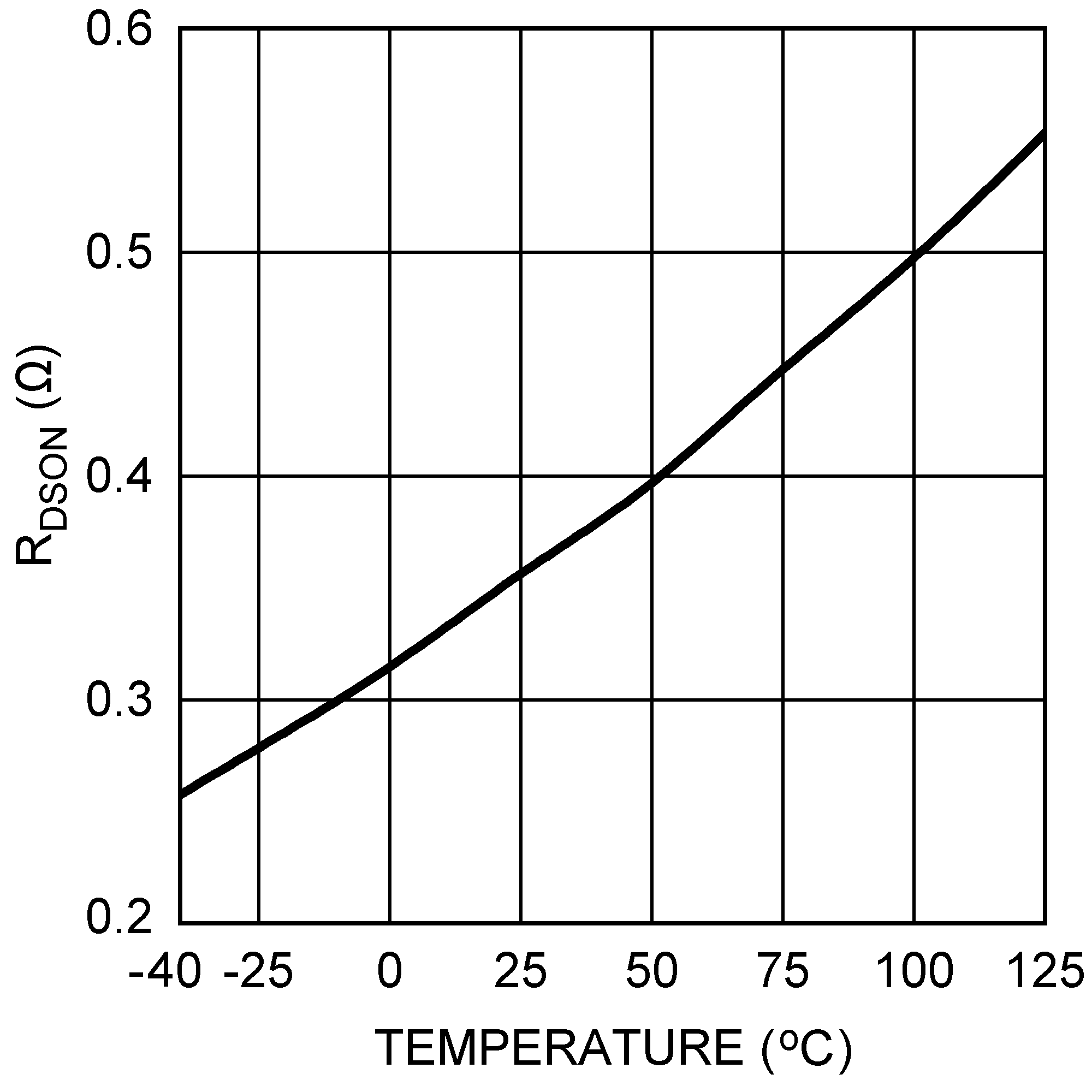
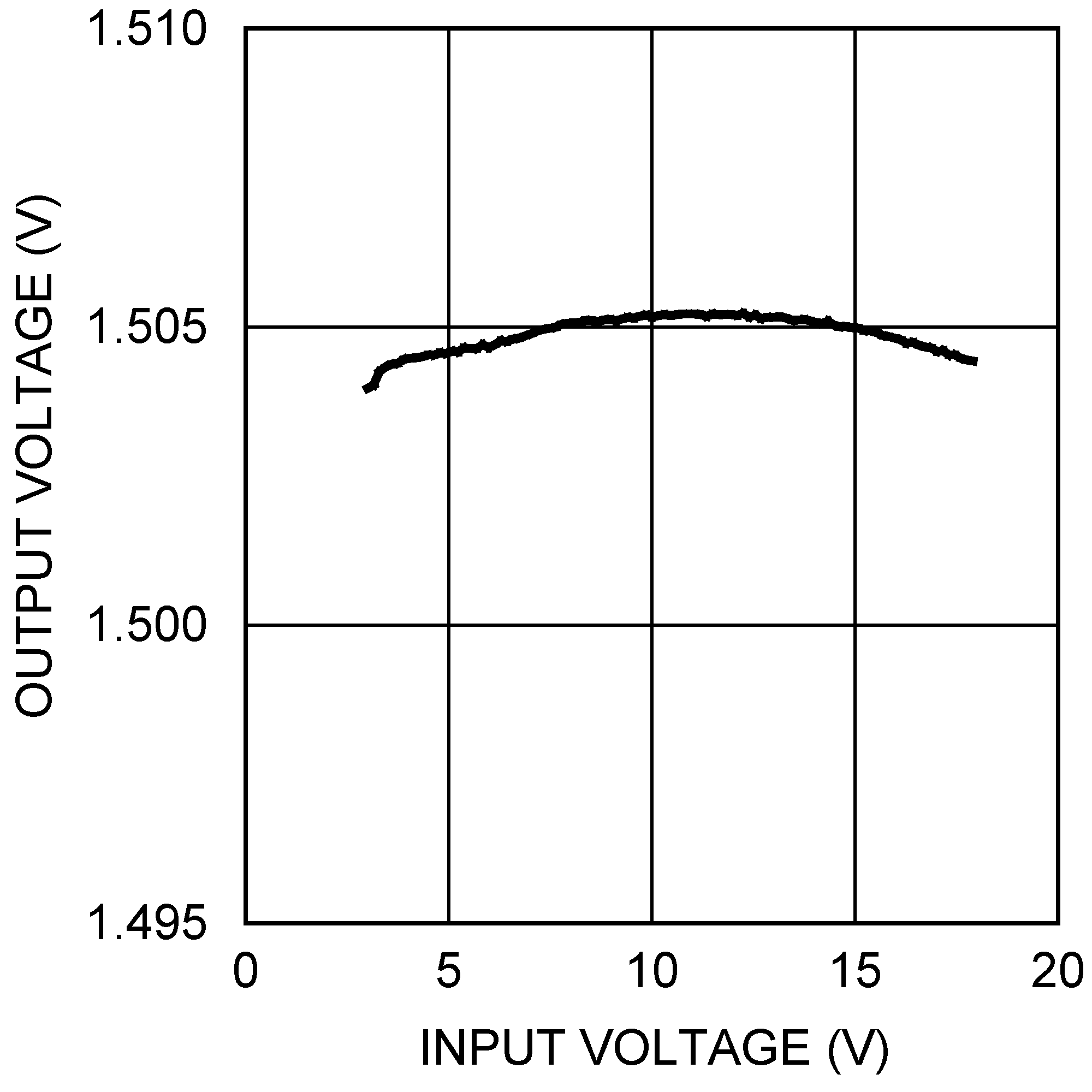
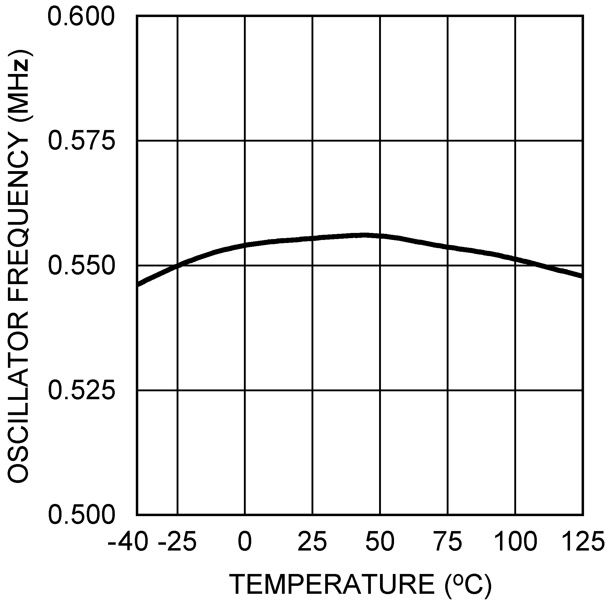
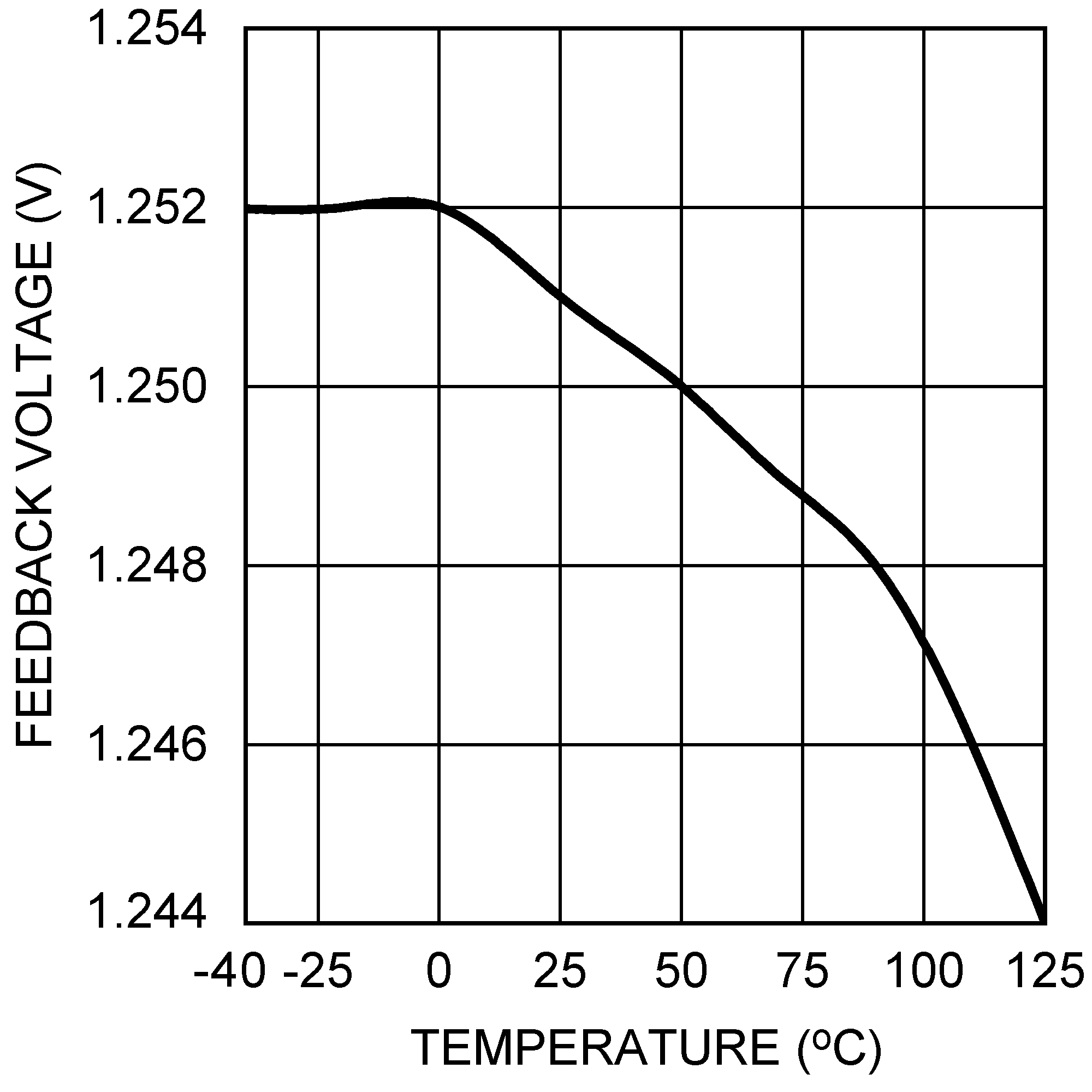
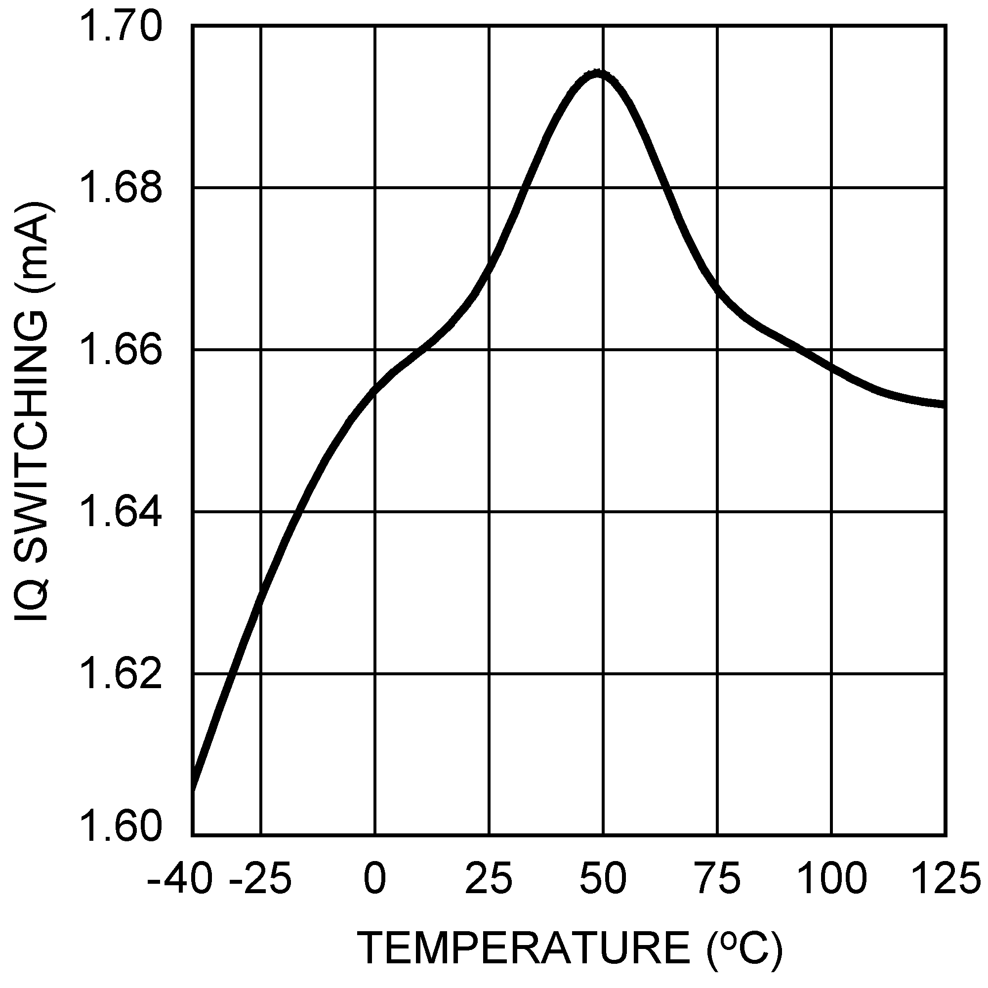
6.6 Typical Characteristics
All curves taken at VIN = 5V, VBOOST - VSW = 5V, L1 = 4.7 µH ("X"), L1 = 10 µH ("Y"), and TA = 25°C, unless specified otherwise.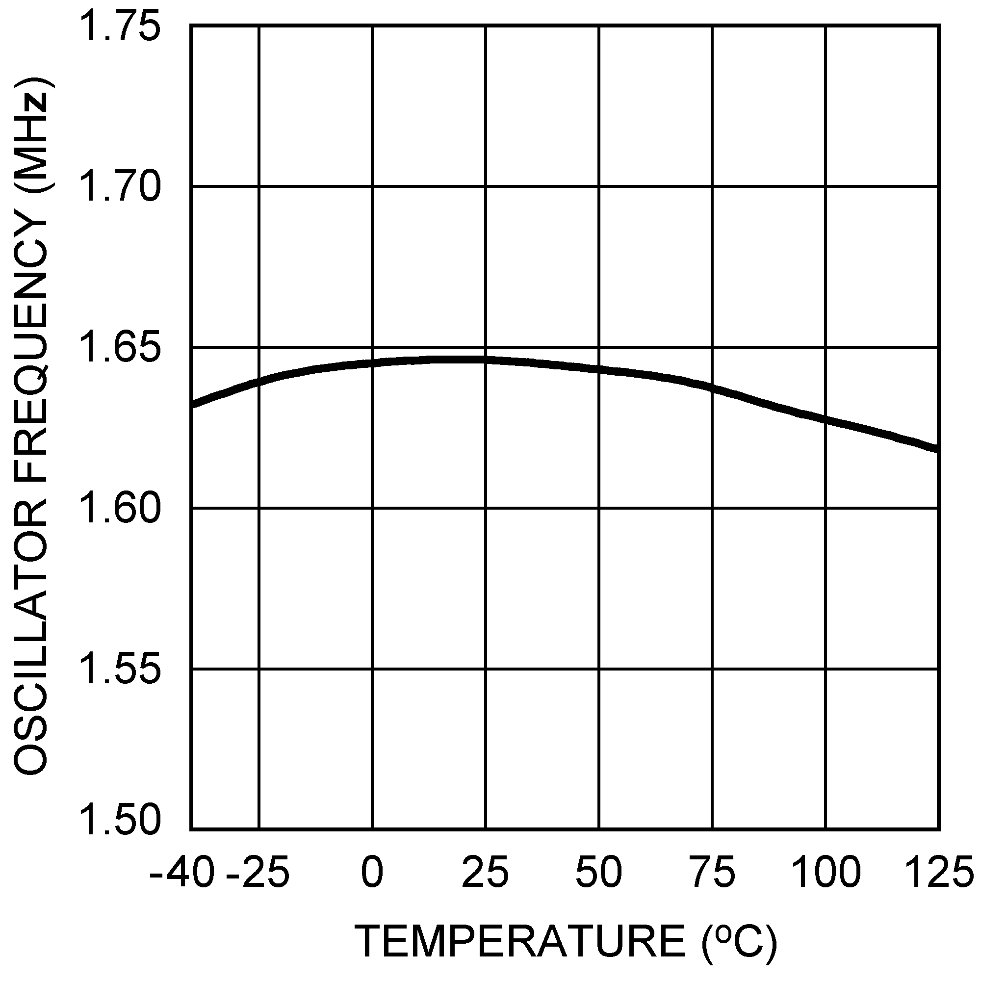
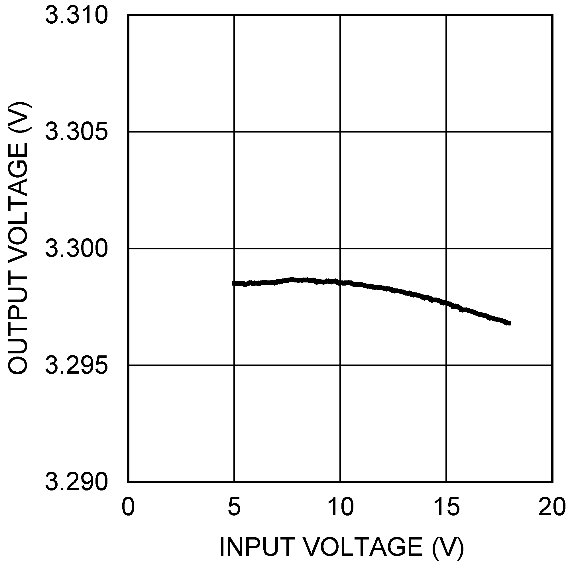
| VOUT = 3.3 V, IOUT = 500 mA |
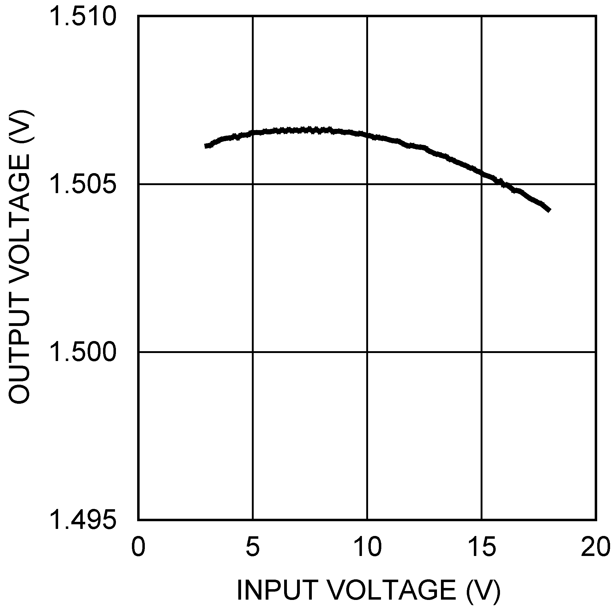
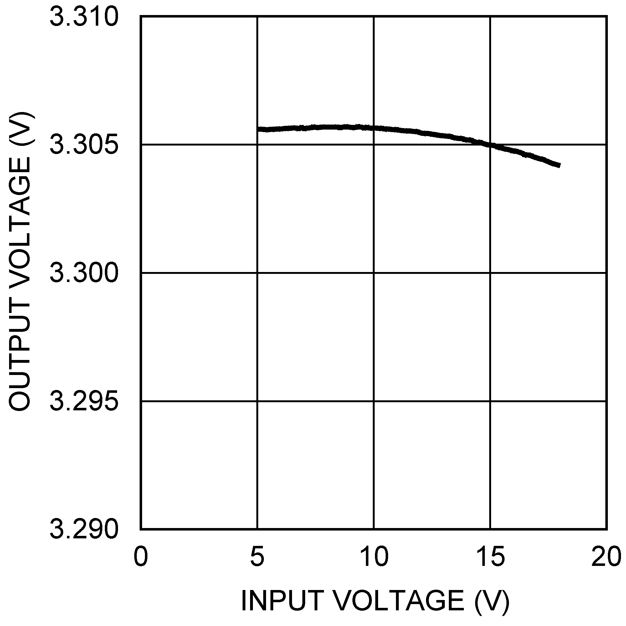
| VOUT = 3.3 V, IOUT = 500 mA |