SNVS136L September 1998 – June 2016 LM2672
PRODUCTION DATA.
- 1 Features
- 2 Applications
- 3 Description
- 4 Revision History
- 5 Description (continued)
- 6 Pin Configuration and Functions
-
7 Specifications
- 7.1 Absolute Maximum Ratings
- 7.2 ESD Ratings
- 7.3 Recommended Operating Conditions
- 7.4 Thermal Information
- 7.5 Electrical Characteristics - 3.3 V
- 7.6 Electrical Characteristics - 5 V
- 7.7 Electrical Characteristics - 12 V
- 7.8 Electrical Characteristics - Adjustable
- 7.9 Electrical Characteristics - All Output Voltage Versions
- 7.10 Typical Characteristics
- 7.11 Typical Characteristics - Fixed Output Voltage Versions
- 8 Parameter Measurement Information
- 9 Detailed Description
-
10Application and Implementation
- 10.1 Application Information
- 10.2
Typical Applications
- 10.2.1 Typical Application for Fixed Output Voltage Versions
- 10.2.2 Typical Application for Adjustable Output Voltage Versions
- 11Power Supply Recommendations
- 12Layout
- 13Device and Documentation Support
- 14Mechanical, Packaging, and Orderable Information
封装选项
机械数据 (封装 | 引脚)
散热焊盘机械数据 (封装 | 引脚)
订购信息
12 Layout
12.1 Layout Guidelines
Layout is very important in switching regulator designs. Rapidly switching currents associated with wiring inductance can generate voltage transients which can cause problems. For minimal inductance and ground loops, the wires indicated by heavy lines (in Figure 19) must be wide printed circuit traces and must be kept as short as possible. For best results, external components must be placed as close to the switcher IC as possible using ground plane construction or single point grounding.
This is the ground reference connection for all components in the power supply. In fast-switching, high-current applications such as those implemented with the LM2672, TI recommends that a broad ground plane be used to minimize signal coupling throughout the circuit.
If open-core inductors are used, take special care as to the location and positioning of this type of inductor. Allowing the inductor flux to intersect sensitive feedback, IC ground path, and COUT wiring can cause problems.
When using the adjustable version, take special care as to the location of the feedback resistors and the associated wiring. Physically place both resistors near the IC, and route the wiring away from the inductor, especially an open core type of inductor.
12.1.1 WSON Package Devices
The LM2672 is offered in the 16-pin WSON surface mount package to allow for increased power dissipation compared to the 8-pin SOIC and PDIP.
The Die Attach Pad (DAP) can and must be connected to PCB Ground plane/island. For CAD and assembly guidelines, refer to AN-1187 Leadless Leadframe Package (LLP).
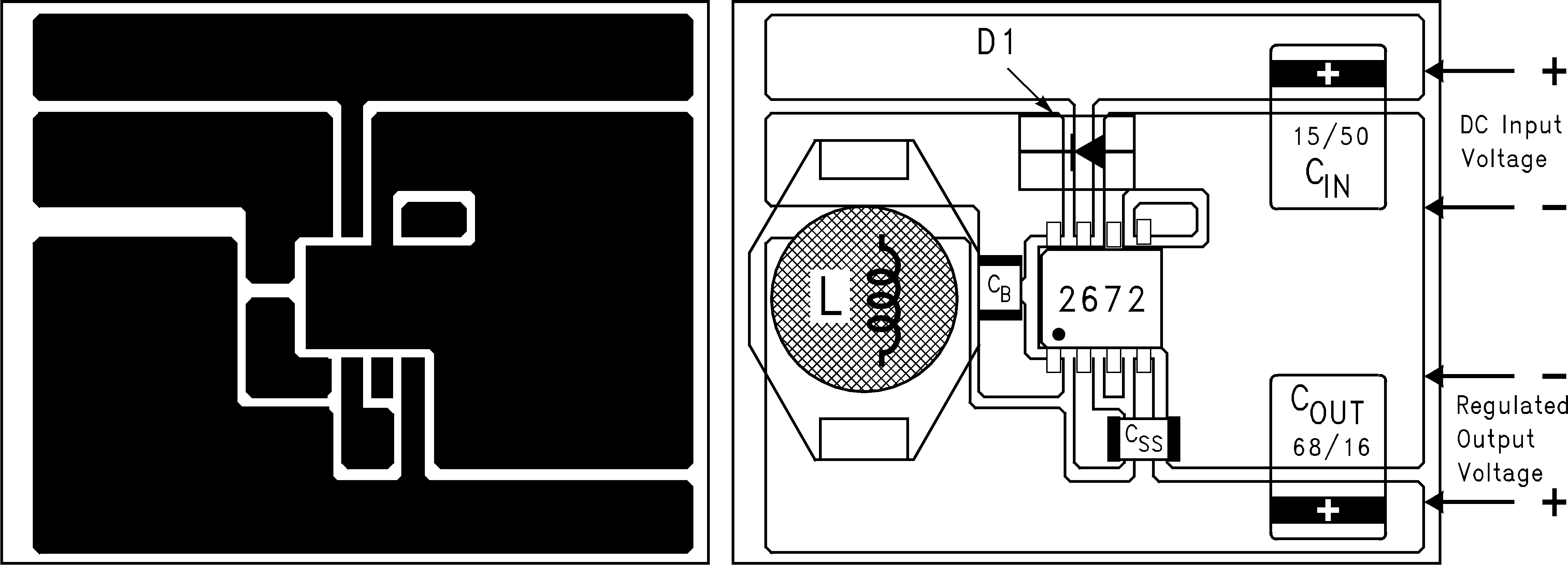
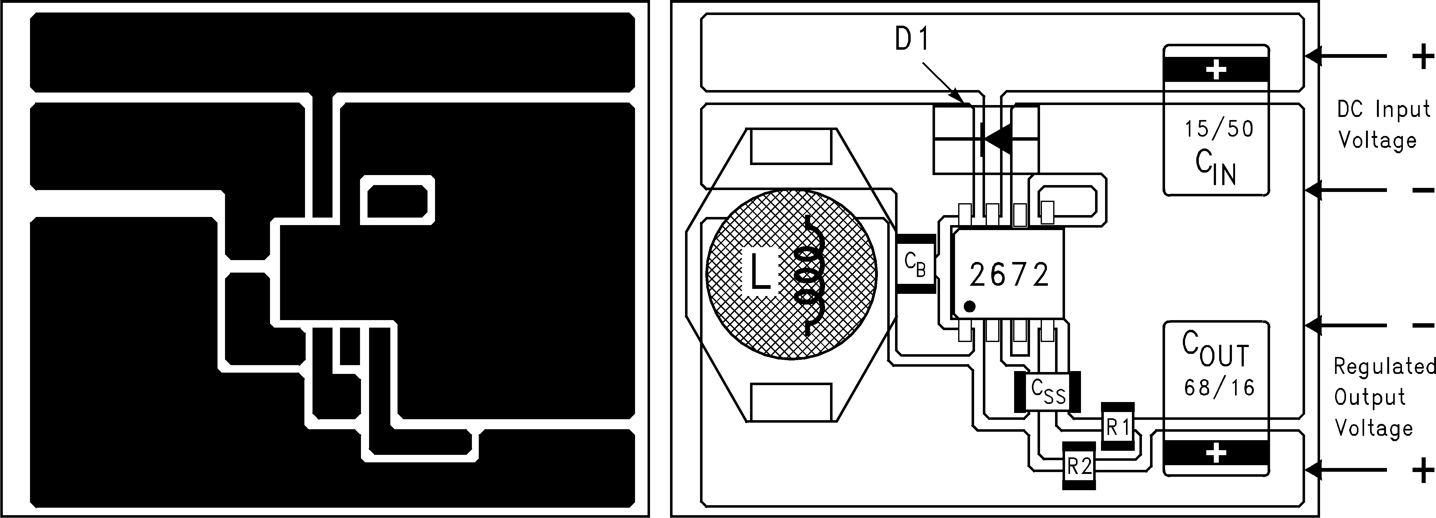
12.2 Layout Examples

| CIN = 15-μF, 50-V, solid tantalum Sprague 594D series | ||
| COUT = 68-μF, 16-V, solid tantalum Sprague 594D series | ||
| D1 = 1-A, 40-V Schottky rectifier, surface mount | ||
| L1 = 33-μH, L23, coilcraft DO3316 | ||
| CB = 0.01-μF, 50-V ceramic | ||

| CIN = 15-μF, 50-V, solid tantalum Sprague 594D series | ||
| COUT = 33-μF, 25-V, solid tantalum Sprague 594D series | ||
| D1 = 1-A, 40-V Schottky rectifier, surface mount | ||
| L1 = 68-μH, L30, coilcraft DO3316 | ||
| CB = 0.01-μF, 50-V ceramic | ||
| R1 = 1k, 1%, R2: use formula in Detailed Design Procedure | ||