SNVS009H November 1999 – March 2016 LM2665
PRODUCTION DATA.
- 1 Features
- 2 Applications
- 3 Description
- 4 Revision History
- 5 Pin Configuration and Functions
- 6 Specifications
- 7 Parameter Measurement Information
- 8 Detailed Description
- 9 Application and Implementation
- 10Power Supply Recommendations
- 11Layout
- 12Device and Documentation Support
- 13Mechanical, Packaging, and Orderable Information
1 Features
- Input Voltage for Voltage Doubler: 2.5 V to 5.5 V
- Voltage Divider Splits Voltage: 1.8 V to 11 V
- Doubles or Splits Input Supply Voltage
- 12-Ω Typical Output Impedance
- 90% Typical Conversion Efficiency at 40 mA
- 1-µA Typical Shutdown Current
2 Applications
- Cellular Phones
- Pagers
- PDAs
- Operational Amplifier Power Suppliers
- Interface Power Suppliers
- Handheld Instruments
- Fire Detection and Notification
- Industrial Handheld Radios
- Blood Pressure Monitors
3 Description
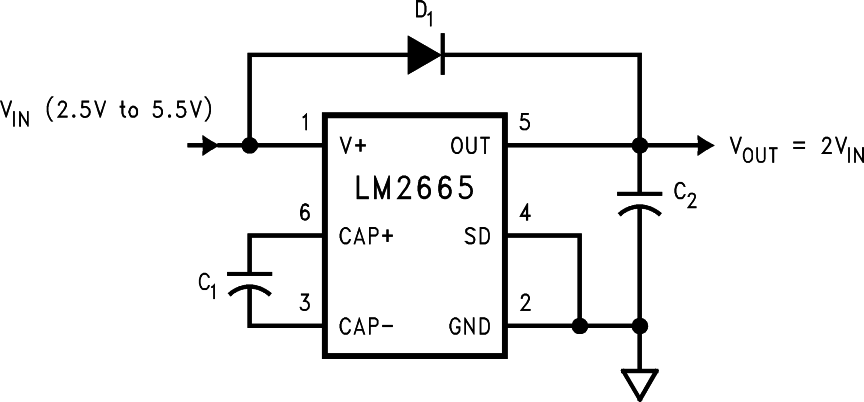
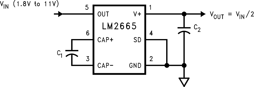
The LM2665 CMOS charge-pump voltage converter operates as a voltage doubler for an input voltage in the range of 2.5 V to 5.5 V. Two low-cost capacitors and a diode (needed during start-up) are used in this circuit to provide up to 40 mA of output current. The LM2665 can also work as a voltage divider to split a voltage in the range of 1.8 V to 11 V in half.
The LM2665 operates at 160-kHz oscillator frequency to reduce output resistance and voltage ripple. With an operating current of only 650 µA (operating efficiency greater than 90% with most loads) and
1-µA typical shutdown current, the LM2665 provides ideal performance for battery powered systems.
Device Information(1)
| PART NUMBER | PACKAGE | BODY SIZE (NOM) |
|---|---|---|
| LM2665 | SOT-23 (6) | 2.90 mm × 1.60 mm |
- For all available packages, see the orderable addendum at the end of the data sheet.
Voltage Doubler

Splitting Vin in Half
