ZHCSGG8F July 2011 – March 2018 LM25118
PRODUCTION DATA.
- 1 特性
- 2 应用
- 3 说明
- 4 修订历史记录
- 5 Pin Configuration and Functions
- 6 Specifications
- 7 Detailed Description
-
8 Application and Implementation
- 8.1 Application Information
- 8.2
Typical Application
- 8.2.1 Design Requirements
- 8.2.2
Detailed Design Procedure
- 8.2.2.1 Custom Design With WEBENCH® Tools
- 8.2.2.2 R7 = RT
- 8.2.2.3 Inductor Selection – L1
- 8.2.2.4 R13 = RSENSE
- 8.2.2.5 C15 = CRAMP
- 8.2.2.6 Inductor Current Limit Calculation
- 8.2.2.7 C9 - C12 = Output Capacitors
- 8.2.2.8 D1
- 8.2.2.9 D4
- 8.2.2.10 C1 – C5 = Input Capacitors
- 8.2.2.11 C20
- 8.2.2.12 C8
- 8.2.2.13 C16 = CSS
- 8.2.2.14 R8, R9
- 8.2.2.15 R1, R3, C21
- 8.2.2.16 R2
- 8.2.2.17 Snubber
- 8.2.2.18 Error Amplifier Configuration
- 8.2.3 Application Curves
- 9 Power Supply Recommendations
- 10Layout
- 11器件和文档支持
- 12机械、封装和可订购信息
9.1 Bias Power Dissipation Reduction
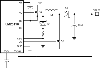
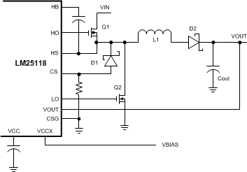
Buck or Buck-boost regulators operating with high-input voltage can dissipate an appreciable amount of power while supplying the required bias current of the IC. The VCC regulator must step-down the input voltage VIN to a nominal VCC level of 7 V. The large voltage drop across the VCC regulator translates into high power dissipation in the VCC regulator. There are several techniques that can significantly reduce this bias regulator power dissipation. Figure 27 and Figure 28 depict two methods to bias the IC, one from the output voltage and one from a separate bias supply. In the first case, the internal VCC regulator is used to initially bias the VCC pin. After the output voltage is established, the VCC pin bias current is supplied through the VCCX pin, which effectively disables the internal VCC regulator. Any voltage greater than 4 V can supply VCC bias through the VCCX pin. However, the voltage applied to the VCCX pin should never exceed 15 V. The voltage supplied through VCCX must be large enough to drive the switching MOSFETs into full saturation.
 Figure 27. VCC Bias From VOUT 4 V < VOUT < 15 V
 Figure 28. VCC Bias With Additional Bias Supply