ZHCSGG8F July 2011 – March 2018 LM25118
PRODUCTION DATA.
- 1 特性
- 2 应用
- 3 说明
- 4 修订历史记录
- 5 Pin Configuration and Functions
- 6 Specifications
- 7 Detailed Description
-
8 Application and Implementation
- 8.1 Application Information
- 8.2
Typical Application
- 8.2.1 Design Requirements
- 8.2.2
Detailed Design Procedure
- 8.2.2.1 Custom Design With WEBENCH® Tools
- 8.2.2.2 R7 = RT
- 8.2.2.3 Inductor Selection – L1
- 8.2.2.4 R13 = RSENSE
- 8.2.2.5 C15 = CRAMP
- 8.2.2.6 Inductor Current Limit Calculation
- 8.2.2.7 C9 - C12 = Output Capacitors
- 8.2.2.8 D1
- 8.2.2.9 D4
- 8.2.2.10 C1 – C5 = Input Capacitors
- 8.2.2.11 C20
- 8.2.2.12 C8
- 8.2.2.13 C16 = CSS
- 8.2.2.14 R8, R9
- 8.2.2.15 R1, R3, C21
- 8.2.2.16 R2
- 8.2.2.17 Snubber
- 8.2.2.18 Error Amplifier Configuration
- 8.2.3 Application Curves
- 9 Power Supply Recommendations
- 10Layout
- 11器件和文档支持
- 12机械、封装和可订购信息
7.3.2 Oscillator and Sync Capability
The LM25118 oscillator frequency is set by a single external resistor connected between the RT pin and the AGND pin. The RT resistor should be located very close to the device and connected directly to the pins of the IC. To set a desired oscillator frequency (f), the necessary value for the RT resistor can be calculated from Equation 1:

The SYNC pin can be used to synchronize the internal oscillator to an external clock. The external clock must be of higher frequency than the free-running frequency set by the RT resistor. A clock circuit with an open-drain output is the recommended interface from the external clock to the SYNC pin. The clock pulse duration should be greater than 15 ns.
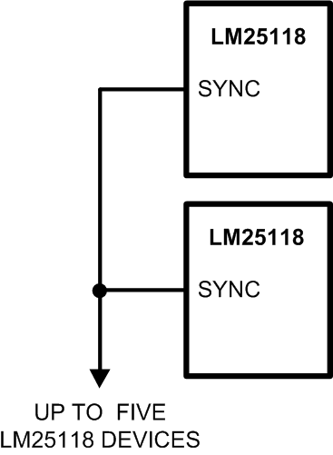
 Figure 11. Sync From Multiple Devices
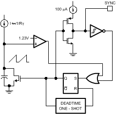
Multiple LM25118 devices can be synchronized together simply by connecting the SYNC pins together. In this configuration, all of the devices will be synchronized to the highest frequency device. The diagram in Figure 11 shows the SYNC input and output features of the LM25118. The internal oscillator circuit drives the SYNC pin with a strong pulldown and weak pullup inverter. When the SYNC pin is pulled low, either by the internal oscillator or an external clock, the ramp cycle of the oscillator is terminated and forced 400 ns off-time is initiated before a new oscillator cycle begins. If the SYNC pins of several LM25118 ICs are connected together, the IC with the highest internal clock frequency will pull all the connected SYNC pins low and terminate the oscillator ramp cycles of the other ICs. The LM25118 with the highest programmed clock frequency will serve as the master and control the switching frequency of all the devices with lower oscillator frequencies.
 Figure 12. Simplified Oscillator and Block Diagram With Sync I/O Circuit