ZHCSIM4H April   2009  – November 2014 LM25011 , LM25011-Q1

PRODUCTION DATA.  

  1. 特性
  2. 应用
  3. 说明
    1.     典型应用
  4. 修订历史记录
  5. Pin Configuration and Functions
    1.     Pin Functions
  6. Specifications
    1. 6.1 Absolute Maximum Ratings
    2. 6.2 Handling Ratings: LM25011
    3. 6.3 Handling Ratings: LM25011-Q1
    4. 6.4 Recommended Operating Conditions
    5. 6.5 Thermal Information
    6. 6.6 Electrical Characteristics
    7. 6.7 Typical Characteristics
  7. Detailed Description
    1. 7.1 Overview
    2. 7.2 Functional Block Diagram
    3. 7.3 Feature Description
      1. 7.3.1 Control Circuit Overview
      2. 7.3.2 On-Time Timer
      3. 7.3.3 Current Limit
      4. 7.3.4 Ripple Requirements
      5. 7.3.5 N-Channel Buck Switch and Driver
      6. 7.3.6 Soft-Start
      7. 7.3.7 Power Good Output (PGD)
      8. 7.3.8 Thermal Shutdown
    4. 7.4 Device Functional Modes
      1. 7.4.1 Shutdown Function
  8. Application and Implementation
    1. 8.1 Application Information
    2. 8.2 Typical Application
      1. 8.2.1 LM25011 Example Circuit
        1. 8.2.1.1 Design Requirements
        2. 8.2.1.2 Detailed Design Procedure
          1. 8.2.1.2.1 Custom Design with WEBENCH Tools
          2. 8.2.1.2.2 External Components
        3. 8.2.1.3 Application Curves
      2. 8.2.2 Output Ripple Control
        1. 8.2.2.1 Option A: Lowest Cost Configuration
        2. 8.2.2.2 Option B: Intermediate VOUT Ripple Configuration
        3. 8.2.2.3 Option C: Minimum VOUT Ripple Configuration
  9. Power Supply Recommendations
  10. 10Layout
    1. 10.1 Layout Guidelines
    2. 10.2 Layout Example
    3. 10.3 Power Dissipation
  11. 11器件和文档支持
    1. 11.1 使用 WEBENCH 工具创建定制设计
    2. 11.2 接收文档更新通知
    3. 11.3 相关链接
    4. 11.4 商标
    5. 11.5 静电放电警告
    6. 11.6 术语表
  12. 12机械、封装和可订购信息

封装选项

机械数据 (封装 | 引脚)
散热焊盘机械数据 (封装 | 引脚)
订购信息

Option B: Intermediate VOUT Ripple Configuration

This configuration generates less ripple at VOUT than Option A by the addition of capacitor (Cff) as shown in Figure 23.

Because the output ripple is passed by Cff to the FB pin with little or no attenuation, the R1 value and VOUT ripple can be smaller than in Option A. The minimum value for R1 is calculated from:

Equation 24. LM25011 LM25011-Q1 LM25011A LM25011A-Q1 30094642.gif

where ΔI is the minimum ripple current amplitude, which occurs at minimum VIN, and VRIPPLE is the peak-to-peak ripple voltage injected at the FB pin. The minimum value for Cff is calculated from:

Equation 25. LM25011 LM25011-Q1 LM25011A LM25011A-Q1 30094643.gif

where tON(max) is the maximum on-time (at minimum VIN), and RFB1//RFB2 is the parallel equivalent of the feedback resistors.
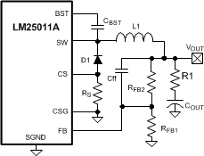
LM25011 LM25011-Q1 LM25011A LM25011A-Q1 30094641.gifFigure 23. Option B – Intermediate Ripple Configuration