ZHCSSA3 october   2021 IWR2243

PRODUCTION DATA  

  1.   1
  2. 特性
  3. 应用
  4. 说明
  5. 功能方框图
  6. Revision History
  7. Device Comparison
    1. 6.1 Related Products
  8. Terminal Configuration and Functions
    1. 7.1 Pin Diagram
    2. 7.2 Signal Descriptions
  9. Specifications
    1. 8.1 Absolute Maximum Ratings
    2. 8.2 ESD Ratings
    3. 8.3 Power-On Hours (POH)
    4. 8.4 Recommended Operating Conditions
    5. 8.5 Power Supply Specifications
    6. 8.6 Power Consumption Summary
    7. 8.7 RF Specification
    8. 8.8 Thermal Resistance Characteristics for FCBGA Package [ABL0161]
    9. 8.9 Timing and Switching Characteristics
      1. 8.9.1 Power Supply Sequencing and Reset Timing
      2. 8.9.2 Synchronized Frame Triggering
      3. 8.9.3 Input Clocks and Oscillators
        1. 8.9.3.1 Clock Specifications
      4. 8.9.4 Multibuffered / Standard Serial Peripheral Interface (MibSPI)
        1. 8.9.4.1 Peripheral Description
          1. 8.9.4.1.1 SPI Timing Conditions
          2. 8.9.4.1.2 SPI Peripheral Mode Switching Parameters (SPICLK = input, SPISIMO = input, and SPISOMI = output)
          3. 8.9.4.1.3 SPI Peripheral Mode Timing Requirements (SPICLK = input, SPISIMO = input, and SPISOMI = output)
        2. 8.9.4.2 Typical Interface Protocol Diagram (Peripheral Mode)
      5. 8.9.5 Inter-Integrated Circuit Interface (I2C)
        1. 8.9.5.1 I2C Timing Requirements
      6. 8.9.6 Quad Serial Peripheral Interface (QSPI)
        1. 8.9.6.1 QSPI Timing Conditions
        2. 8.9.6.2 Timing Requirements for QSPI Input (Read) Timings
        3. 8.9.6.3 QSPI Switching Characteristics
      7. 8.9.7 LVDS Interface Configuration
        1. 8.9.7.1 LVDS Interface Timings
      8. 8.9.8 General-Purpose Input/Output
        1. 8.9.8.1 Switching Characteristics for Output Timing versus Load Capacitance (CL)
      9. 8.9.9 Camera Serial Interface (CSI)
        1. 8.9.9.1 CSI Switching Characteristics
  10. Detailed Description
    1. 9.1 Overview
    2. 9.2 Functional Block Diagram
    3. 9.3 Subsystems
      1. 9.3.1 RF and Analog Subsystem
        1. 9.3.1.1 Clock Subsystem
        2. 9.3.1.2 Transmit Subsystem
        3. 9.3.1.3 Receive Subsystem
      2. 9.3.2 Host Interface
    4. 9.4 Other Subsystems
      1. 9.4.1 ADC Data Format Over CSI2 Interface
      2. 9.4.2 ADC Channels (Service) for User Application
        1. 9.4.2.1 GPADC Parameters
  11. 10Monitoring and Diagnostic Mechanisms
  12. 11Applications, Implementation, and Layout
    1. 11.1 Application Information
    2. 11.2 Imaging Radar using Cascade Configuration
    3. 11.3 Reference Schematic
    4. 11.4 Layout
      1. 11.4.1 Layout Guidelines
      2. 11.4.2 Stackup Details
  13. 12Device and Documentation Support
    1. 12.1 Device Nomenclature
    2. 12.2 Tools and Software
    3. 12.3 Documentation Support
    4. 12.4 支持资源
    5. 12.5 Trademarks
    6. 12.6 静电放电警告
    7. 12.7 Export Control Notice
    8. 12.8 术语表
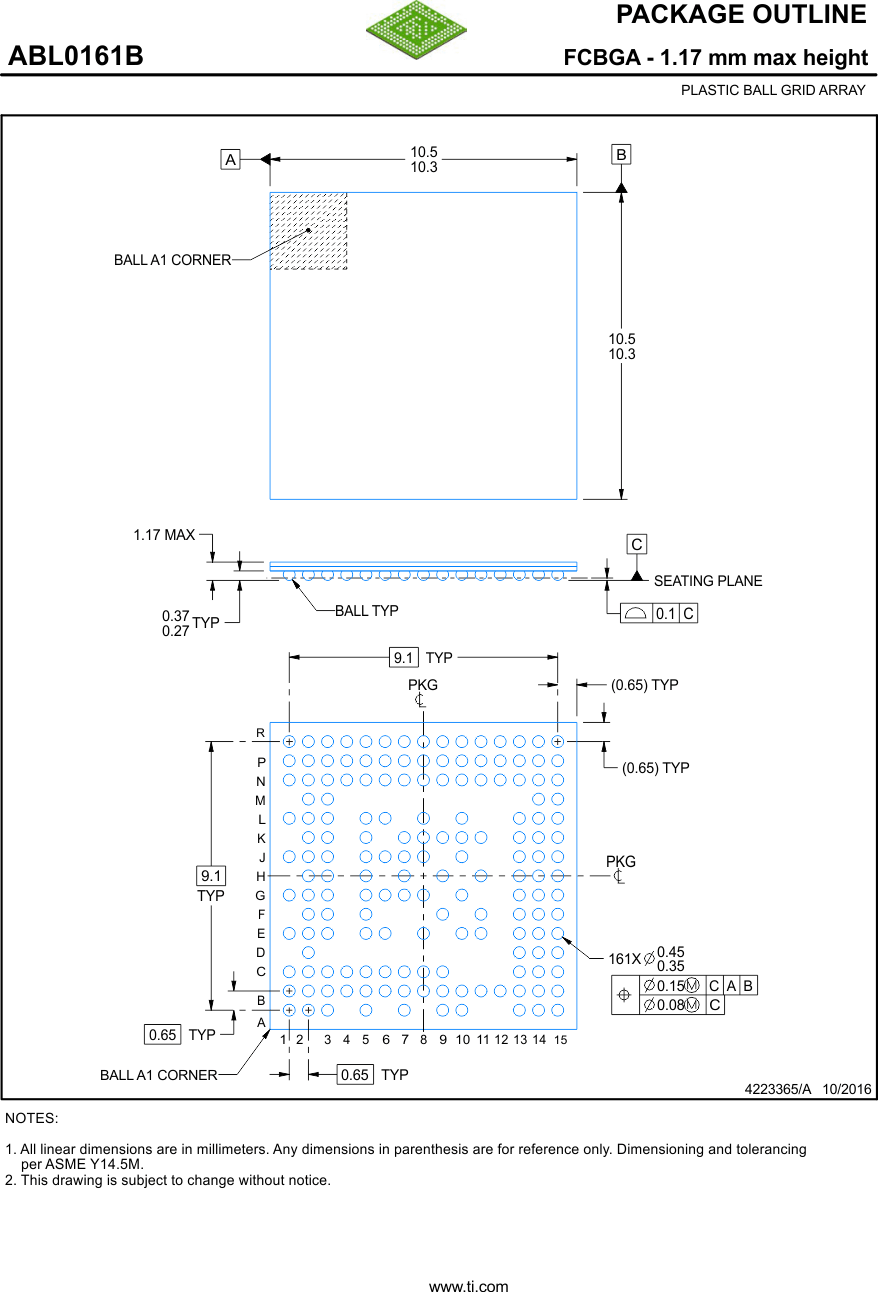
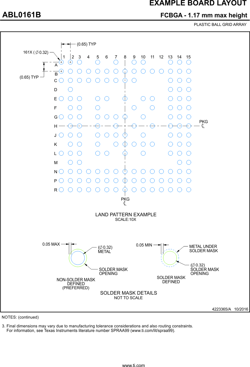
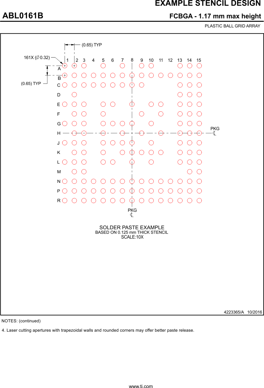
  14. 13Mechanical, Packaging, and Orderable Information
    1. 13.1 Packaging Information

封装选项

机械数据 (封装 | 引脚)
散热焊盘机械数据 (封装 | 引脚)
订购信息

Packaging Information

The following pages include mechanical, packaging, and orderable information. This information is the most current data available for the designated devices. This data is subject to change without notice and revision of this document. For browser-based versions of this data sheet, refer to the left-hand navigation.

CAUTION:

The following package information is subject to change without notice.

GUID-45A021B8-DE81-41C7-B605-F68683B23203-low.gif
GUID-74F7380A-19C8-40B7-BF9D-51FAAF57BC07-low.gif
GUID-5F9373AB-758E-4139-B093-D0662757FC4A-low.gif