ZHCSIE0A June 2018 – October 2018 ISO224
PRODUCTION DATA.
- 1 特性
- 2 应用
- 3 说明
- 4 修订历史记录
- 5 器件比较表
- 6 Pin Configuration and Functions
-
7 Specifications
- 7.1 Absolute Maximum Ratings
- 7.2 ESD Ratings
- 7.3 Recommended Operating Conditions
- 7.4 Thermal Information
- 7.5 Power Ratings
- 7.6 Insulation Specifications
- 7.7 Safety-Related Certifications
- 7.8 Safety Limiting Values
- 7.9 Electrical Characteristics
- 7.10 Switching Characteristics
- 7.11 Insulation Characteristics Curves
- 7.12 Typical Characteristics
- 8 Detailed Description
- 9 Application and Implementation
- 10Power Supply Recommendations
- 11Layout
- 12器件和文档支持
- 13机械、封装和可订购信息
10 Power Supply Recommendations
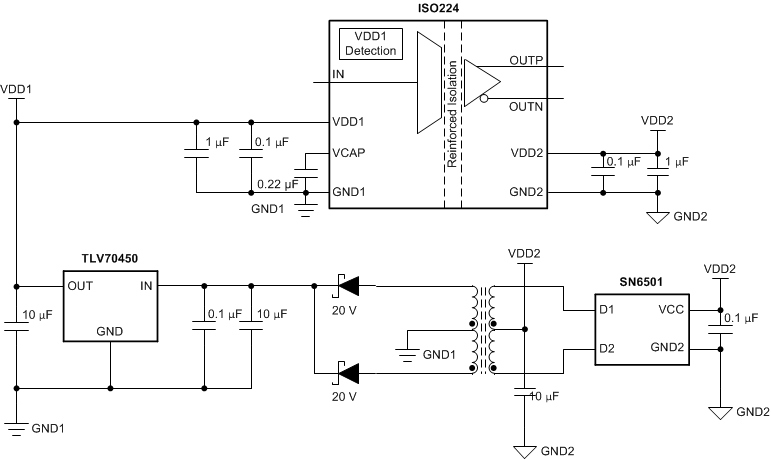
In a typical application, the high-side power supply (VDD1) for the ISO224 is generated from the low-side supply (VDD2) of the device by an isolated DC/DC converter circuit. A low-cost solution is based on the push-pull driver SN6501 and a transformer that supports the desired isolation voltage ratings. TI recommends using a low-ESR decoupling capacitor of 0.1 µF and an additional capacitor of a minimum 1 µF for both supplies of the ISO224. Figure 51 shows the recommended placement of these decoupling capacitors as close as possible to the ISO224 power-supply pins to minimize supply current loops and electromagnetic emissions.
To decouple the output of the integrated LDO, use a 0.22-µF capacitor placed as close to the VCAP pin of the ISO224 as possible.
The ISO224 does not require any specific power up sequencing. Consider the analog settling time tAS as specified in the Switching Characteristics table after ramp up of the VDD1 high-side supply.
 Figure 51. SN6501-Based, High-Side Power Supply