ZHCSGR1A August   2017  – January 2018 INA828

PRODUCTION DATA.  
  1. 特性
  2. 应用
  3. 说明
    1.     Device Images
      1.      INA828 简化内部原理图
      2.      输入失调电压漂移的典型分布
  4. 修订历史记录
  5. Pin Configuration and Functions
    1.     Pin Functions
  6. Specifications
    1. 6.1 Absolute Maximum Ratings
    2. 6.2 ESD Ratings
    3. 6.3 Recommended Operating Conditions
    4. 6.4 Thermal Information
    5. 6.5 Electrical Characteristics
    6. 6.6 Typical Characteristics
  7. Detailed Description
    1. 7.1 Overview
    2. 7.2 Functional Block Diagram
    3. 7.3 Feature Description
      1. 7.3.1 Setting the Gain
        1. 7.3.1.1 Gain Drift
      2. 7.3.2 EMI Rejection
        1. Table 2. INA828 EMIRR for Frequencies of Interest
      3. 7.3.3 Input Common-Mode Range
      4. 7.3.4 Input Protection
      5. 7.3.5 Operating Voltage
    4. 7.4 Device Functional Modes
  8. Application and Implementation
    1. 8.1 Reference Terminal
    2. 8.2 Input Bias Current Return Path
    3. 8.3 PCB Assembly Effects on Precision
    4. 8.4 Typical Application
      1. 8.4.1 Design Requirements
      2. 8.4.2 Detailed Design Procedure
      3. 8.4.3 Application Curves
    5. 8.5 Other Application Examples
      1. 8.5.1 Resistance Temperature Detector Interface
  9. Power Supply Recommendations
  10. 10Layout
    1. 10.1 Layout Guidelines
    2. 10.2 Layout Example
  11. 11器件和文档支持
    1. 11.1 Documentation Support
      1. 11.1.1 Related Documentation
    2. 11.2 Receiving Notification of Documentation Updates
    3. 11.3 Community Resources
    4. 11.4 商标
    5. 11.5 静电放电警告
    6. 11.6 Glossary
  12. 12机械、封装和可订购信息

封装选项

机械数据 (封装 | 引脚)
散热焊盘机械数据 (封装 | 引脚)
订购信息

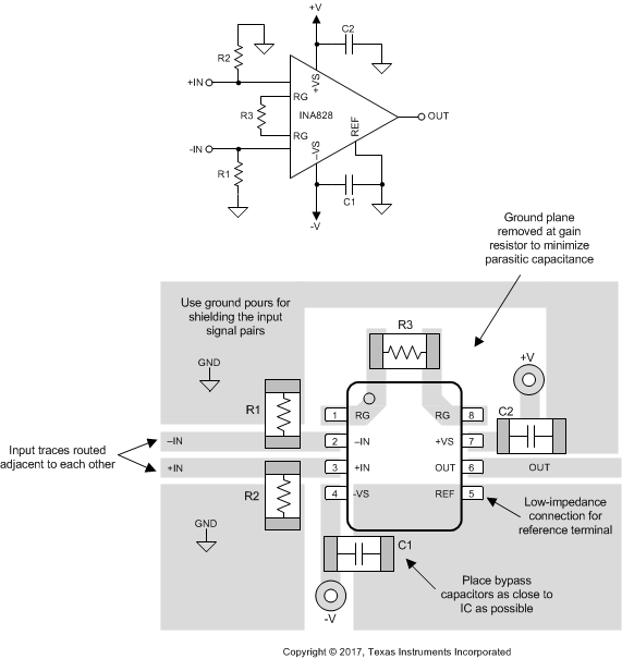
Layout Example

INA828 PCBLayout_SBOS792.gifFigure 74. Example Schematic and Associated PCB Layout