ZHCSK07A July 2019 – January 2021 INA253-Q1
PRODUCTION DATA
- 1 特性
- 2 应用
- 3 说明
- 4 Revision History
- 5 Pin Configuration and Functions
- 6 Specifications
-
7 Detailed Description
- 7.1 Overview
- 7.2 Functional Block Diagram
- 7.3 Feature Description
- 7.4
Device Functional Modes
- 7.4.1 Adjusting the Output Midpoint With the Reference Pins
- 7.4.2 Reference Pin Connections for Unidirectional Current Measurements
- 7.4.3 Ground Referenced Output
- 7.4.4 Reference Pin Connections for Bidirectional Current Measurements
- 7.4.5 Output Set to Mid-Supply Voltage
- 7.4.6 Output Set to Mid-External Reference
- 7.4.7 Output Set Using Resistor Divide
- 8 Application and Implementation
- 9 Power Supply Recommendations
- 10Layout
- 11Device and Documentation Support
- 12Mechanical, Packaging, and Orderable Information
6.6 Typical Characteristics
at TA = 25 °C, VS = 5 V, VIN+ = 12 V, and VREF = VS / 2 (unless otherwise noted)
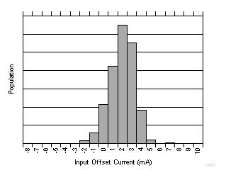
| All gains |

| All gains |
 Figure 6-5 Power-Supply Rejection Ratio vs Temperature
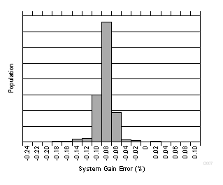 Figure 6-7 Gain Error Production Distribution (INA253A2-Q1)
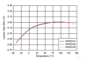 Figure 6-9 System Gain Error vs Temperature
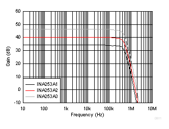
| VCM = 0 V, VDIFF = 10-mVPP sine |
 Figure 6-13 Common-Mode Rejection Ratio vs Frequency
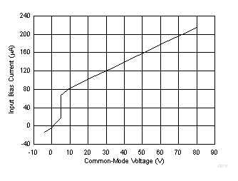
| VS = 5 V |
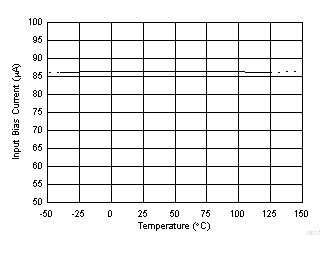 Figure 6-17 Input Bias Current vs Temperature
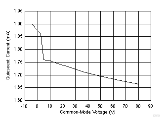 Figure 6-19 Quiescent Current vs Common-mode Voltage
 Figure 6-21 INA253A2-Q1 Input-Referred Voltage Noise vs Frequency
 Figure 6-23 0.1-Hz to 10-Hz Voltage Noise (Referred-to-Input)
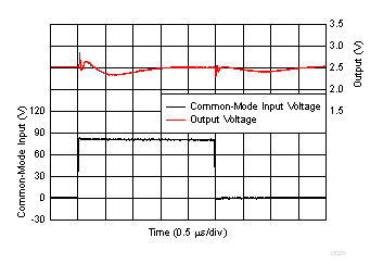
| VREF1 = VREF2 = 0 V |

| Rising Edge |
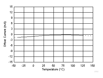 Figure 6-2 Input Offset Current vs Temperature
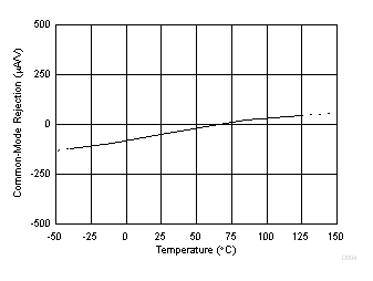 Figure 6-4 Common-Mode Rejection Ratio vs Temperature
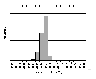 Figure 6-6 Gain
Error Production Distribution (INA253A1-Q1)
 Figure 6-8 Gain Error Production Distribution (INA253A3-Q1)
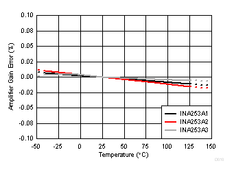 Figure 6-10 Amplifier Gain Error vs Temperature
 Figure 6-12 Power-Supply Rejection Ratio vs Frequency
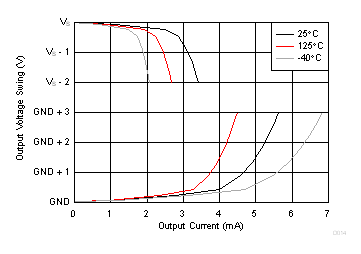
| VS = 5 V | ||
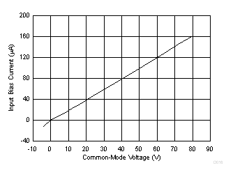
| VS = 0 V | ||
 Figure 6-18 Quiescent Current vs Temperature
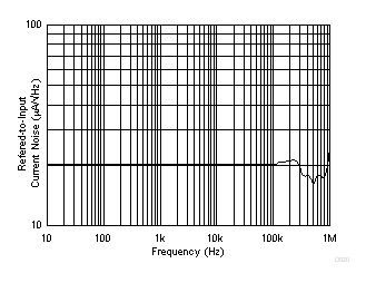 Figure 6-20 INA253A1-Q1 Input-Referred Voltage Noise vs Frequency
 Figure 6-22 INA253A3-Q1 Input-Referred Voltage Noise vs Frequency
| VREF1 = VREF2 = 0 V, 10-mVPP input step |
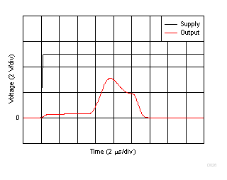 Figure 6-26 Start-Up Response
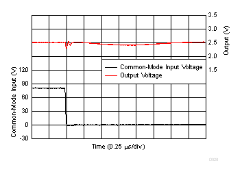
| Falling Edge |