ZHCSFN7E June   2009  – January 2016 INA220

PRODUCTION DATA.  

  1. 特性
  2. 应用范围
  3. 说明
  4. 修订历史记录
  5. Related Products
  6. Pin Configuration and Functions
  7. Specifications
    1. 7.1 Absolute Maximum Ratings
    2. 7.2 ESD Ratings
    3. 7.3 Recommended Operating Conditions
    4. 7.4 Thermal Information
    5. 7.5 Electrical Characteristics
    6. 7.6 Bus Timing Diagram Definitions
    7. 7.7 Typical Characteristics
  8. Detailed Description
    1. 8.1 Overview
    2. 8.2 Functional Block Diagram
    3. 8.3 Feature Description
      1. 8.3.1 Basic ADC Functions
        1. 8.3.1.1 Power Measurement
        2. 8.3.1.2 PGA Function
        3. 8.3.1.3 Compatibility With TI Hot Swap Controllers
    4. 8.4 Device Functional Modes
      1. 8.4.1 Filtering and Input Considerations
    5. 8.5 Programming
      1. 8.5.1 Programming the INA220 Calibration Register
      2. 8.5.2 Programming the INA220 Power Measurement Engine
        1. 8.5.2.1 Calibration Register and Scaling
      3. 8.5.3 Simple Current Shunt Monitor Usage (No Programming Necessary)
      4. 8.5.4 Bus Overview
        1. 8.5.4.1 Serial Bus Address
        2. 8.5.4.2 Serial Interface
      5. 8.5.5 Writing to and Reading from the INA220
        1. 8.5.5.1 High-Speed Two-Wire Mode
        2. 8.5.5.2 Power-Up Conditions
    6. 8.6 Register Maps
      1. 8.6.1 Register Information
      2. 8.6.2 Register Details
        1. 8.6.2.1 Configuration Register (address = 00h) [reset = 399Fh]
      3. 8.6.3 Data Output Registers
        1. 8.6.3.1 Shunt Voltage Register (address = 01h)
        2. 8.6.3.2 Bus Voltage Register (address = 02h)
        3. 8.6.3.3 Power Register (address = 03h) [reset = 00h]
        4. 8.6.3.4 Current Register (address = 04h) [reset =00h]
      4. 8.6.4 Calibration Register
        1. 8.6.4.1 Calibration Register (address = 05h) [reset = 00h]
  9. Application and Implementation
    1. 9.1 Application Information
    2. 9.2 Typical Application
      1. 9.2.1 Design Requirements
      2. 9.2.2 Detailed Design Procedure
        1. 9.2.2.1 Register Results for the Example Circuit
      3. 9.2.3 Typical Application: -48-V Telecom Current/Voltage/Power Sense With Isolation
      4. 9.2.4 Typical Application: 48-V Telecom Current/Voltage/Power Sense
      5. 9.2.5 Typical Application: General Source Low-Side Sensing
  10. 10Power Supply Recommendations
  11. 11Layout
    1. 11.1 Layout Guidelines
    2. 11.2 Layout Example
  12. 12器件和文档支持
    1. 12.1 相关文档 
    2. 12.2 社区资源
    3. 12.3 商标
    4. 12.4 静电放电警告
    5. 12.5 Glossary
  13. 13机械、封装和可订购信息

封装选项

机械数据 (封装 | 引脚)
散热焊盘机械数据 (封装 | 引脚)
订购信息

Layout

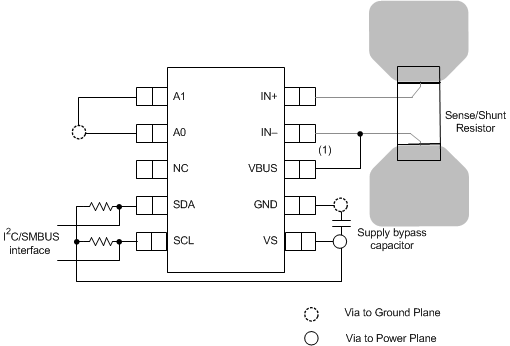
Layout Guidelines

Connect the input pins (IN+ and IN–) to the sensing resistor using a Kelvin connection or a 4-wire connection. These connection techniques ensure that only the current-sensing resistor impedance is detected between the input pins. Poor routing of the current-sensing resistor commonly results in additional resistance present between the input pins. Given the very low ohmic value of the current-sensing resistor, any additional high-current carrying impedance causes significant measurement errors. Place the power-supply bypass capacitor as close as possible to the supply and ground pins.

Layout Example

INA220 ai_recommended-layout_sbos459.gif
(1) Connect the VBUS pin to the power supply rail
Figure 34. Layout Recommendation