ZHCSFN4E November   2006  – September 2017 INA200 , INA201 , INA202

PRODUCTION DATA.  

  1. 特性
  2. 应用
  3. 说明
  4. 修订历史记录
  5. Pin Configuration and Functions
  6. Specifications
    1. 6.1 Absolute Maximum Ratings
    2. 6.2 ESD Ratings
    3. 6.3 Recommended Operating Conditions
    4. 6.4 Thermal Information
    5. 6.5 Electrical Characteristics: Current-Shunt Monitor
    6. 6.6 Electrical Characteristics: Comparator
    7. 6.7 Electrical Characteristics: General
    8. 6.8 Typical Characteristics
  7. Detailed Description
    1. 7.1 Overview
    2. 7.2 Functional Block Diagram
    3. 7.3 Feature Description
      1. 7.3.1 Basic Connections
      2. 7.3.2 Selecting RS
      3. 7.3.3 Comparator
    4. 7.4 Device Functional Modes
      1. 7.4.1 Input Filtering
      2. 7.4.2 Accuracy Variations as a Result of VSENSE and Common-Mode Voltage
        1. 7.4.2.1 Normal Case 1: VSENSE ≥ 20 mv, VCM ≥ VS
        2. 7.4.2.2 Normal Case 2: VSENSE ≥ 20 mv, VCM < VS
        3. 7.4.2.3 Low VSENSE Case 1: VSENSE < 20 mV, -16 V ≤ VCM < 0 and Low VSENSE Case 3: VSENSE < 20 mV, VS < VCM ≤ 80 V
        4. 7.4.2.4 Low VSENSE Case 2: VSENSE < 20 mV, 0 V ≤ VCM ≤ VS
      3. 7.4.3 Transient Protection
      4. 7.4.4 Output Voltage Range
  8. Application and Implementation
    1. 8.1 Application Information
    2. 8.2 Typical Application
      1. 8.2.1 Design Requirements
      2. 8.2.2 Detailed Design Procedure
      3. 8.2.3 Application Curve
  9. Power Supply Recommendations
    1. 9.1 Output vs Supply Ramp Considerations
  10. 10Layout
    1. 10.1 Layout Guidelines
    2. 10.2 Layout Example
  11. 11器件和文档支持
    1. 11.1 相关链接
    2. 11.2 社区资源
    3. 11.3 商标
    4. 11.4 静电放电警告
    5. 11.5 Glossary
  12. 12机械、封装和可订购信息

封装选项

机械数据 (封装 | 引脚)
散热焊盘机械数据 (封装 | 引脚)
订购信息

Layout

Layout Guidelines

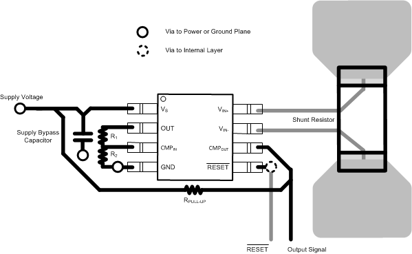
  • Connect the input pins to the sensing resistor using a Kelvin or 4-wire connection. This connection technique ensures that only the current-sensing resistor impedance is detected between the input pins. Poor routing of the current-sensing resistor commonly results in additional resistance present between the input pins. Given the very-low-ohmic value of the current resistor, any additional high-current carrying impedance causes significant measurement errors.
  • The power-supply bypass capacitor must be placed as close as possible to the supply and ground pins. The recommended value of this bypass capacitor is 0.1 μF. Additional decoupling capacitance can be added to compensate for noisy or high-impedance power supplies.

Layout Example

INA200 INA201 INA202 pcblayout.gif Figure 39. INA20x Layout Example