ZHCSFN4E November   2006  – September 2017 INA200 , INA201 , INA202

PRODUCTION DATA.  

  1. 特性
  2. 应用
  3. 说明
  4. 修订历史记录
  5. Pin Configuration and Functions
  6. Specifications
    1. 6.1 Absolute Maximum Ratings
    2. 6.2 ESD Ratings
    3. 6.3 Recommended Operating Conditions
    4. 6.4 Thermal Information
    5. 6.5 Electrical Characteristics: Current-Shunt Monitor
    6. 6.6 Electrical Characteristics: Comparator
    7. 6.7 Electrical Characteristics: General
    8. 6.8 Typical Characteristics
  7. Detailed Description
    1. 7.1 Overview
    2. 7.2 Functional Block Diagram
    3. 7.3 Feature Description
      1. 7.3.1 Basic Connections
      2. 7.3.2 Selecting RS
      3. 7.3.3 Comparator
    4. 7.4 Device Functional Modes
      1. 7.4.1 Input Filtering
      2. 7.4.2 Accuracy Variations as a Result of VSENSE and Common-Mode Voltage
        1. 7.4.2.1 Normal Case 1: VSENSE ≥ 20 mv, VCM ≥ VS
        2. 7.4.2.2 Normal Case 2: VSENSE ≥ 20 mv, VCM < VS
        3. 7.4.2.3 Low VSENSE Case 1: VSENSE < 20 mV, -16 V ≤ VCM < 0 and Low VSENSE Case 3: VSENSE < 20 mV, VS < VCM ≤ 80 V
        4. 7.4.2.4 Low VSENSE Case 2: VSENSE < 20 mV, 0 V ≤ VCM ≤ VS
      3. 7.4.3 Transient Protection
      4. 7.4.4 Output Voltage Range
  8. Application and Implementation
    1. 8.1 Application Information
    2. 8.2 Typical Application
      1. 8.2.1 Design Requirements
      2. 8.2.2 Detailed Design Procedure
      3. 8.2.3 Application Curve
  9. Power Supply Recommendations
    1. 9.1 Output vs Supply Ramp Considerations
  10. 10Layout
    1. 10.1 Layout Guidelines
    2. 10.2 Layout Example
  11. 11器件和文档支持
    1. 11.1 相关链接
    2. 11.2 社区资源
    3. 11.3 商标
    4. 11.4 静电放电警告
    5. 11.5 Glossary
  12. 12机械、封装和可订购信息

封装选项

机械数据 (封装 | 引脚)
散热焊盘机械数据 (封装 | 引脚)
订购信息

Power Supply Recommendations

The input circuitry of the INA20x devices can accurately measure beyond the power-supply voltage, Vs. For example, the Vs power supply is 5 V, whereas the load power-supply voltage is up to 80 V. However, the output voltage range of the OUT pin is limited by the voltages on the power supply pin.

Output vs Supply Ramp Considerations

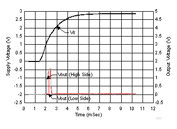
Figure 36, Figure 37, and Figure 38 show the typical output voltages for high and low-side configurations with the given ramp supply voltage. These fluctuations on the output during power-up may require a controller to incorporate a blanking time to disregard the artifacts.
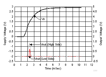
INA200 INA201 INA202 D200_SBOS374.gif Figure 36. Analog Output vs Supply Ramp (INA200)
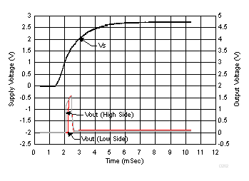
INA200 INA201 INA202 D202_SBOS374.gif Figure 38. Analog Output vs Supply Ramp (INA202)
INA200 INA201 INA202 D201_SBOS374.gif Figure 37. Analog Output vs Supply Ramp (INA201)