ZHCSHW3D March   2018  – November 2019 INA190

PRODUCTION DATA.  

  1. 特性
  2. 应用
  3. 说明
    1.     Device Images
      1.      典型应用
  4. 修订历史记录
  5. Pin Configuration and Functions
    1.     Pin Functions
  6. Specifications
    1. 6.1 Absolute Maximum Ratings
    2. 6.2 ESD Ratings
    3. 6.3 Recommended Operating Conditions
    4. 6.4 Thermal Information
    5. 6.5 Electrical Characteristics
    6. 6.6 Typical Characteristics
  7. Detailed Description
    1. 7.1 Overview
    2. 7.2 Functional Block Diagram
    3. 7.3 Feature Description
      1. 7.3.1 Precision Current Measurement
      2. 7.3.2 Low Input Bias Current
      3. 7.3.3 Low Quiescent Current With Output Enable
      4. 7.3.4 Bidirectional Current Monitoring
      5. 7.3.5 High-Side and Low-Side Current Sensing
      6. 7.3.6 High Common-Mode Rejection
      7. 7.3.7 Rail-to-Rail Output Swing
    4. 7.4 Device Functional Modes
      1. 7.4.1 Normal Operation
      2. 7.4.2 Unidirectional Mode
      3. 7.4.3 Bidirectional Mode
      4. 7.4.4 Input Differential Overload
      5. 7.4.5 Shutdown
  8. Application and Implementation
    1. 8.1 Application Information
      1. 8.1.1 Basic Connections
      2. 8.1.2 RSENSE and Device Gain Selection
      3. 8.1.3 Signal Conditioning
      4. 8.1.4 Common-Mode Voltage Transients
    2. 8.2 Typical Applications
      1. 8.2.1 Design Requirements
      2. 8.2.2 Detailed Design Procedure
      3. 8.2.3 Application Curve
  9. Power Supply Recommendations
  10. 10Layout
    1. 10.1 Layout Guidelines
    2. 10.2 Layout Examples
  11. 11器件和文档支持
    1. 11.1 文档支持
      1. 11.1.1 相关文档
    2. 11.2 接收文档更新通知
    3. 11.3 支持资源
    4. 11.4 商标
    5. 11.5 静电放电警告
    6. 11.6 Glossary
  12. 12机械、封装和可订购信息

封装选项

机械数据 (封装 | 引脚)
散热焊盘机械数据 (封装 | 引脚)
订购信息

Basic Connections

Figure 39 shows the basic connections of the INA190. Place the device as close as possible to the current sense resistor and connect the input pins (IN+ and IN–) to the current sense resistor through kelvin connections.If present, the ENABLE pin must be controlled externally or connected to VS if not used.
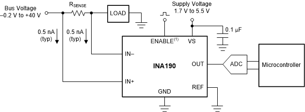
INA190 ina190-typical-application.gif
The ENABLE pin is available only in the DDF and RSW packages.
NOTE: To help eliminate ground offset errors between the device and the analog-to-digital converter (ADC), connect the REF pin to the ADC reference input. When driving SAR ADCs, filter or buffer the output of the INA190 before connecting directly to the ADC.
Figure 39. Basic Connections for the INA190