ZHCSDI9D January 2015 – January 2017 HD3SS460
PRODUCTION DATA.
- 1 特性
- 2 应用
- 3 说明
- 4 修订历史记录
- 5 Device Comparison Table
- 6 Pin Configuration and Functions
- 7 Specifications
- 8 Detailed Description
- 9 Application and Implementation
- 10Power Supply Recommendations
- 11Layout
- 12器件和文档支持
- 13机械、封装和可订购信息
封装选项
请参考 PDF 数据表获取器件具体的封装图。
机械数据 (封装 | 引脚)
- RNH|30
- RHR|28
散热焊盘机械数据 (封装 | 引脚)
- RHR|28
订购信息
6 Pin Configuration and Functions
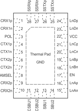
RHR Package With Thermal Pad
(28-Pin WQFN)
Top View

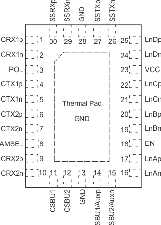
RNH Package With Thermal Pad
(30-Pin WQFN)
Top View

Pin Functions
| PIN | TYPE(1) | DESCRIPTION | ||
|---|---|---|---|---|
| NAME | RHR NO. |
RNH NO. |
||
| VCC | 22 | 23 | P | Power |
| GND | PAD | 13, 28, PAD | G | Ground |
| POL | 3 | 3 | Input | Provides MUX control (Table 1) |
| AMSEL | 8 | 8 | 3-Level Input | Provides MUX configurations (Table 1) |
| EN | 17 | 18 | 3-Level Input | Enable signal; also provides MUX control (Table 1) |
| CRX1p, n | 1, 2 | 1, 2 | I/O | High Speed Signal Port CRX1 positive, negative |
| CTX1p, n | 4, 5 | 4, 5 | I/O | High Speed Signal Port CTX1 positive, negative |
| CTX2p, n | 6, 7 | 6, 7 | I/O | High Speed Signal Port CTX2 positive, negative |
| CRX2p, n | 9, 10 | 9, 10 | I/O | High Speed Signal Port CRX2 positive, negative |
| LnAn, p | 15, 16 | 16, 17 | I/O | High Speed Signal Port LnA positive, negative |
| LnBn, p | 18, 19 | 19, 20 | I/O | High Speed Signal Port LnB negative, positive |
| LnCn, p | 20, 21 | 21, 22 | I/O | High Speed Signal Port LnC negative, positive |
| LnDn, p | 23, 24 | 24, 25 | I/O | High Speed Signal Port LnD negative, positive |
| SSTXn, p | 25, 26 | 26, 27 | I/O | High Speed Signal Port SSTX negative, positive |
| SSRXn, p | 27, 28 | 29, 30 | I/O | High Speed Signal Port SSRX negative, positive |
| CSBU1, 2 | 11, 12 | 11, 12 | I/O | Low Speed Signal Port CSBU 1, 2 |
| SBU1, 2 | 13, 14 | 14, 15 | I/O | Low Speed Signal Port SBU 1, 2 |
(1) High speed data ports (CRX[1/2][p/n], Ln[A-D][p,n], and SS[T/R]X[p/n]) incorporate 20kΩ pull down resistors that are switched in when a port is not selected and switched out when the port is selected.