ZHCSEC8 November 2015 HD3SS3411
PRODUCTION DATA.
8 Application Information and Implementation
NOTE
Information in the following applications sections is not part of the TI component specification, and TI does not warrant its accuracy or completeness. TI’s customers are responsible for determining suitability of components for their purposes. Customers should validate and test their design implementation to confirm system functionality.
8.1 Application Information
HD3SS3411 mux channels have independent adaptive common mode tracking allowing RX and TX paths to have different common mode voltage simplifying system implementation and avoiding inter-operational issues.
HD3SS3411 mux does not provide common mode biasing for the channel. Therefore, it is required that the device is biased from either side for all active channels.
The HD3SS3411 supports several high-speed data protocols with a differential amplitude of < 1800 mVpp and a common mode voltage of < 2 V, as with USB 3.1 and DisplayPort 1.3. The one select input (SEL) pin can be controlled by an available GPIO pin within a system or from a microcontroller.
8.2 Typical Application
 Figure 3. FPD Link III Application
8.3 Design Requirements
For this design example, use the values shown in Table 3.
Table 3. Design Paramerters
| PARAMETER | VALUE |
|---|---|
| VCC voltage | 3.3 V |
| Ap/n, Bp/n, Cp/n CM input voltage | 0 V to 2 V |
| SEL/OEn pin max voltage for low | 0 V |
| SEL/OEn pin min voltage for high | 3.3 V |
8.4 Detailed Design Procedure
8.4.1 AC Coupling Capacitors
Many interfaces require AC coupling between the transmitter and receiver. The 0402 capacitors are the preferred option to provide AC coupling, and the 0603 size capacitors will also work. The 0805 size capacitors and C-packs should be avoided. When placing AC coupling capacitors symmetric placement is best. A capacitor value of 0.1 µF is best and the value should be match for the ± signal pair. The placement should be along the TX pairs on the system board, which are usually routed on the top layer of the board.
There are several placement options for the AC coupling capacitors. Because the switch requires a bias voltage, the capacitors must only be placed on one side of the switch. If they are placed on both sides of the switch, a biasing voltage should be provided. A few placement options are shown below. In Figure 4, the coupling capacitors are placed between the switch and endpoint. In this situation, the switch is biased by the system/host controller.
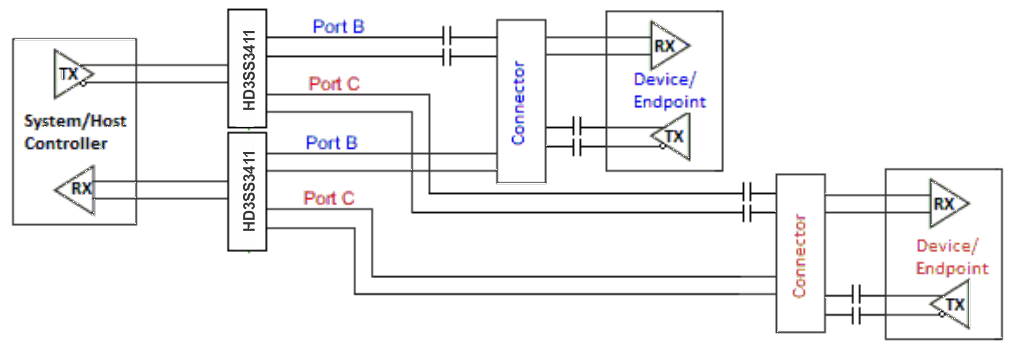 Figure 4. AC Coupling Capacitors Between Switch TX and Endpoint TX
In Figure 5, the coupling capacitors are placed on the host transmit pair and endpoint transmit pair. In this situation, the switch on the top is biased by the endpoint and the lower switch is biased by the host controller.
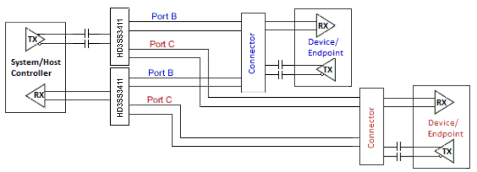 Figure 5. AC Coupling Capacitors on Host TX and Endpoint TX
If the common mode voltage in the system is higher than 2 V, the coupling capacitors are placed on both sides of the switch (shown in Figure 6). A biasing voltage of less than 2 V is required in this case.
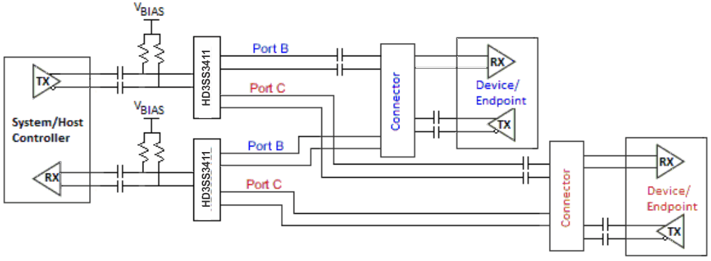 Figure 6. AC Coupling Capacitors on Both Sides of Switch
8.5 Application Curves
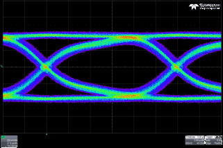 Figure 7. 6 Gbps Source Eye Diagram
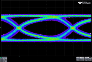 Figure 8. 6 Gbps Output Eye Diagram