ZHCSEC8 November   2015 HD3SS3411

PRODUCTION DATA.  

  1. 特性
  2. 应用
  3. 说明
  4. 修订历史记录
  5. Pin Configuration and Functions
  6. Specifications
    1. 6.1 Absolute Maximum Ratings
    2. 6.2 ESD Ratings
    3. 6.3 Recommended Operating Conditions
    4. 6.4 Thermal Information
    5. 6.5 Electrical Characteristics
    6. 6.6 Timing Requirements
    7. 6.7 Typical Characteristics
  7. Detailed Description
    1. 7.1 Overview
    2. 7.2 Functional Block Diagram
    3. 7.3 Feature Description
      1. 7.3.1 Output Enable and Power Savings
    4. 7.4 Device Functional Modes
  8. Application Information and Implementation
    1. 8.1 Application Information
    2. 8.2 Typical Application
    3. 8.3 Design Requirements
    4. 8.4 Detailed Design Procedure
      1. 8.4.1 AC Coupling Capacitors
    5. 8.5 Application Curves
  9. Power Supply Recommendations
  10. 10Layout
    1. 10.1 Layout Guidelines
      1. 10.1.1 Critical Routes
      2. 10.1.2 General Routing/Placement Rules
    2. 10.2 Layout Example
  11. 11器件和文档支持
    1. 11.1 文档支持
    2. 11.2 社区资源
    3. 11.3 商标
    4. 11.4 静电放电警告
    5. 11.5 Glossary
  12. 12机械、封装和可订购信息

封装选项

机械数据 (封装 | 引脚)
散热焊盘机械数据 (封装 | 引脚)
订购信息

Pin Configuration and Functions

RWA Package
14 Pin (WQFN)
Top View
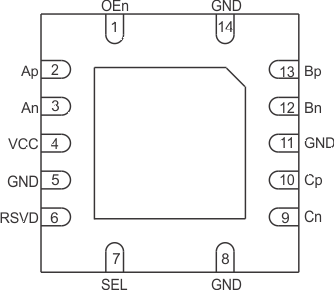
HD3SS3411 po_slase82.gif

Pin Functions

NAME NO TYPE DESCRIPTION
Ap 2 I/O Port A, High Speed Positive Signal
An 3 I/O Port A, High Speed Negative Signal
Bp 13 I/O Port B, High Speed Positive Signal
Bn 12 I/O Port B, High Speed Negative Signal
Cp 10 I/O Port C, High Speed Positive Signal
Cn 9 I/O Port C, High Speed Negative Signal
GND 5,8,11,14, Pad G Ground
OEn 1 I Active Low Chip Enable
L: Normal operation
H: Shutdown
RSVD 6 I/O Reserved Pin – connect or pull-down to GND
SEL 7 I Port select pin
L: Port A to Port B
H: Port A to Port C
VCC 4 P 3.3 V power