ZHCSIL1A July   2018  – December 2018 DSLVDS1001

PRODUCTION DATA.  

  1. 特性
  2. 应用
  3. 说明
    1.     功能图
    2.     典型应用
  4. 修订历史记录
  5. Pin Configuration and Functions
    1.     Pin Functions
  6. Specifications
    1. 6.1 Absolute Maximum Ratings
    2. 6.2 ESD Ratings
    3. 6.3 Recommended Operating Conditions
    4. 6.4 Thermal Information
    5. 6.5 Electrical Characteristics
    6. 6.6 Switching Characteristics
    7. 6.7 Typical Characteristics
  7. Parameter Measurement Information
  8. Detailed Description
    1. 8.1 Overview
    2. 8.2 Functional Block Diagram
    3. 8.3 Feature Description
      1. 8.3.1 DSLVDS1001 Driver Functionality
      2. 8.3.2 Driver Output Voltage and Power-On Reset
      3. 8.3.3 Driver Offset
    4. 8.4 Device Functional Modes
  9. Application and Implementation
    1. 9.1 Application Information
    2. 9.2 Typical Application
      1. 9.2.1 Point-to-Point Communications
    3. 9.3 Design Requirements
    4. 9.4 Detailed Design Procedure
      1. 9.4.1 Driver Supply Voltage
      2. 9.4.2 Driver Bypass Capacitance
      3. 9.4.3 Driver Input Voltage
      4. 9.4.4 Driver Output Voltage
      5. 9.4.5 Interconnecting Media
      6. 9.4.6 PCB Transmission Lines
      7. 9.4.7 Termination Resistor
    5. 9.5 Application Curve
  10. 10Power Supply Recommendations
    1. 10.1 Power Supply Considerations
  11. 11Layout
    1. 11.1 Layout Guidelines
      1. 11.1.1 Microstrip vs. Stripline Topologies
      2. 11.1.2 Dielectric Type and Board Construction
      3. 11.1.3 Recommended Stack Layout
      4. 11.1.4 Separation Between Traces
      5. 11.1.5 Crosstalk and Ground Bounce Minimization
      6. 11.1.6 Decoupling
    2. 11.2 Layout Example
  12. 12器件和文档支持
    1. 12.1 文档支持
      1. 12.1.1 相关文档
    2. 12.2 接收文档更新通知
    3. 12.3 社区资源
    4. 12.4 商标
    5. 12.5 静电放电警告
    6. 12.6 术语表
  13. 13机械、封装和可订购信息

封装选项

机械数据 (封装 | 引脚)
散热焊盘机械数据 (封装 | 引脚)
订购信息

Microstrip vs. Stripline Topologies

As per the LVDS Application and Data Handbook (SLLD009), printed-circuit boards usually offer designers two transmission line options: microstrip and stripline. Microstrips are traces on the outer layer of a PCB, as shown in Figure 15.
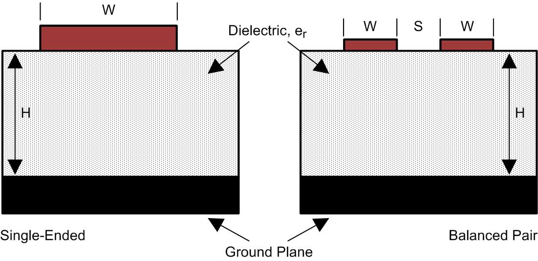
DSLVDS1001 lo_mt_slls373.pngFigure 15. Microstrip Topology

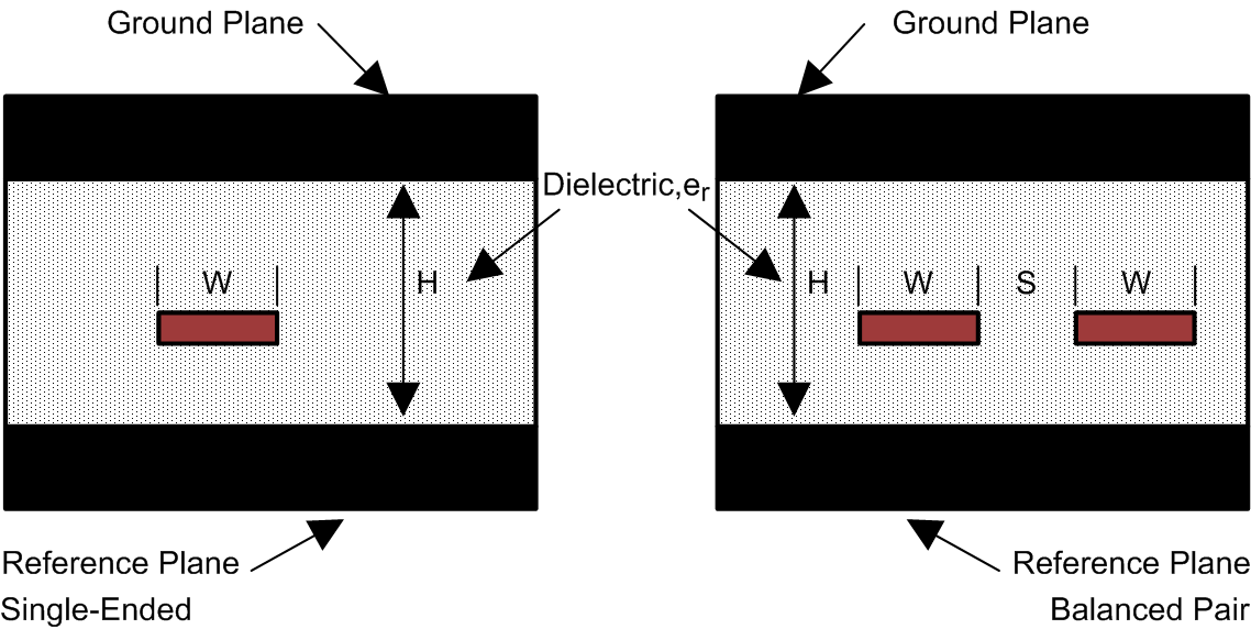
On the other hand, striplines are traces between two ground planes. Striplines are less prone to emissions and susceptibility problems because the reference planes effectively shield the embedded traces. However, from the standpoint of high-speed transmission, juxtaposing two planes creates additional capacitance. TI recommends routing LVDS signals on microstrip transmission lines, if possible. The PCB traces allow designers to specify the necessary tolerances for ZO based on the overall noise budget and reflection allowances. Footnotes 1(2), 2(3), and 3(4) provide formulas for ZO and tPD for differential and single-ended traces. (2)(3)(4)
Howard Johnson & Martin Graham.1993. High Speed Digital Design – A Handbook of Black Magic. Prentice Hall PRT. ISBN number 013395724.
Mark I. Montrose. 1996. Printed Circuit Board Design Techniques for EMC Compliance. IEEE Press. ISBN number 0780311310.
Clyde F. Coombs, Jr. Ed, Printed Circuits Handbook, McGraw Hill, ISBN number 0070127549.

DSLVDS1001 lo_st_slls373.pngFigure 16. Stripline Topology