ZHCSJA8B September   2005  – January 2019 DS90LV049H

PRODUCTION DATA.  

  1. 特性
  2. 应用
  3. 说明
    1.     Device Images
      1.      双列直插式
      2.      功能图
  4. 修订历史记录
  5. Pin Configuration and Functions
    1.     Pin Functions
  6. Specifications
    1. 6.1 Absolute Maximum Ratings
    2. 6.2 ESD Ratings
    3. 6.3 Recommended Operating Conditions
    4. 6.4 Thermal Information
    5. 6.5 Electrical Characteristics
    6. 6.6 Switching Characteristics
    7. 6.7 Typical Characteristics
  7. Parameter Measurement Information
  8. Detailed Description
    1. 8.1 Overview
    2. 8.2 Functional Block Diagram
    3. 8.3 Feature Description
      1. 8.3.1 DS90LV049H LVDS Driver and Receiver Functionality
      2. 8.3.2 Termination
      3. 8.3.3 Fail-Safe Feature
    4. 8.4 Device Functional Modes
  9. Application and Implementation
    1. 9.1 Application Information
    2. 9.2 Typical Application
      1. 9.2.1 Design Requirements
      2. 9.2.2 Detailed Design Procedure
        1. 9.2.2.1 Power Decoupling Recommendations
        2. 9.2.2.2 PCB Transmission Lines
        3. 9.2.2.3 Input Fail-Safe Biasing
        4. 9.2.2.4 Probing LVDS Transmission Lines on PCB
        5. 9.2.2.5 Interconnecting Media
      3. 9.2.3 Application Curve
  10. 10Power Supply Recommendations
  11. 11Layout
    1. 11.1 Layout Guidelines
      1. 11.1.1 Microstrip vs. Stripline Topologies
      2. 11.1.2 Dielectric Type and Board Construction
      3. 11.1.3 Recommended Stack Layout
      4. 11.1.4 Separation Between Traces
      5. 11.1.5 Crosstalk and Ground Bounce Minimization
      6. 11.1.6 Decoupling
    2. 11.2 Layout Example
  12. 12器件和文档支持
    1. 12.1 相关文档
    2. 12.2 接收文档更新通知
    3. 12.3 社区资源
    4. 12.4 商标
    5. 12.5 静电放电警告
    6. 12.6 术语表
  13. 13机械、封装和可订购信息

封装选项

机械数据 (封装 | 引脚)
散热焊盘机械数据 (封装 | 引脚)
订购信息

Pin Configuration and Functions

PW Package
16-Pin TSSOP
Top View
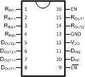
DS90LV049H 20161701.gif

Pin Functions

PIN I/O DESCRIPTION
NAME NO.
DIN 10, 11 I Driver input pins, LVCMOS levels. There is a pulldown current source present.
DOUT+ 6, 7 O Noninverting driver output pins, LVDS levels.
DOUT− 5, 8 O Inverting driver output pins, LVDS levels.
RIN+ 2, 3 I Noninverting receiver input pins, LVDS levels. There is a pullup current source present.
RIN– 1, 4 I Inverting receiver input pins, LVDS levels. There is a pulldown current source present.
ROUT 14, 15 O Receiver output pins, LVCMOS levels.
EN, EN 9, 16 I Enable and Disable pins. There are pulldown current sources present at both pins.
VDD 12 I Power supply pin.
GND 13 I Ground pin.