ZHCSIT3C February 2012 – September 2018 DS90C187
PRODUCTION DATA.
- 1 特性
- 2 应用
- 3 说明
- 4 修订历史记录
- 5 (说明 (续))
- 6 Pin Configuration and Functions
- 7 Specifications
-
8 Detailed Description
- 8.1 Overview
- 8.2 Functional Block Diagrams
- 8.3
Device Functional Modes
- 8.3.1 Device Configuration
- 8.3.2 Single Pixel Input / Single Pixel Output
- 8.3.3 Single Pixel Input / Dual Pixel Output
- 8.3.4 Dual Pixel Input / Dual Pixel Output
- 8.3.5 Pixel Clock Edge Select (RFB)
- 8.3.6 Power Management
- 8.3.7 Sleep Mode (PDB)
- 8.3.8 LVDS Outputs
- 8.3.9 18 bit / 24 bit Color Mode (18B)
- 8.3.10 LVCMOS Inputs
- 8.4 Programming
- 9 Application and Implementation
- 10Power Supply Recommendations
- 11Layout
- 12器件和文档支持
- 13机械、封装和可订购信息
7.8 AC Timing Diagrams
A. The worst case test pattern produces a maximum toggling of digital circuits, LVDS I/O and LVCMOS/ I/O.
Figure 1. Checker Board Test Pattern 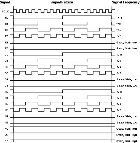
A. The worst case test pattern produces a maximum toggling of digital circuits, LVDS I/O and LVCMOS/ I/O.
B. Recommended pin to signal mapping for 18 bits per pixel, customer may choose to define differently. The 16 grayscale test pattern tests device power consumption for a “typical” LCD display pattern. The test pattern approximates signal switching needed to produce groups of 16 vertical stripes across the display.
C. Figure 2 shows a falling edge data strobe (IN_CLK).
Figure 2. “16 Gray Scale” Test Pattern (Falling Edge Clock shown)  Figure 3. DS90C187 (Transmitter) LVDS Output Load
  Figure 4. LVDS Output Transition Times
  Figure 5. LVCMOS Input Transition Times
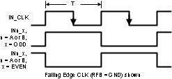
  Figure 6. LVCMOS Input Setup/Hold and Clock High/Low Times (Falling Edge Strobe)
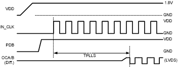
  Figure 8. Sleep Mode / Power Down Delay
 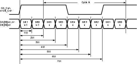 Figure 9. LVDS Serial Bit Positions
 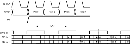 Figure 10. Single In Dual Out Mode Timing and Latency
  Figure 11. Single In Single Out / Dual In Dual Out Latency