ZHCSCZ2A July 2014 – September 2014 DS125BR820
PRODUCTION DATA.
- 1 特性
- 2 应用
- 3 说明
- 4 修订历史记录
- 5 Pin Configuration and Functions
- 6 Specifications
- 7 Detailed Description
- 8 Applications and Implementation
- 9 Power Supply Recommendations
- 10Layout
- 11器件和文档支持
- 12机械封装和可订购信息
6 Specifications
6.1 Absolute Maximum Ratings(1)
over operating free-air temperature range (unless otherwise noted)| MIN | MAX | UNIT | ||
|---|---|---|---|---|
| Supply Voltage (VDD to GND, 2.5 V Mode) | -0.5 | +2.75 | V | |
| Supply Voltage (VIN to GND, 3.3 V Mode) | -0.5 | +4.0 | V | |
| LVCMOS Input/Output Voltage | -0.5 | +4.0 | V | |
| CML Input Voltage | -0.5 | VDD + 0.5 | V | |
| CML Input Current | -30 | +30 | mA | |
(1) “Absolute Maximum Ratings” indicate limits beyond which damage to the device may occur, including inoperability and degradation of device reliability and performance. Functional operation of the device and/or non-degradation at the Absolute Maximum Ratings or other conditions beyond those indicated in the Recommended Operating Conditions is not implied. The Recommended Operating Conditions indicate conditions at which the device is functional and the device should not be operated beyond such conditions. Absolute Maximum Numbers are ensured for a junction temperature range of -40°C to +125°C. Models are validated to Maximum Operating Voltages only.
6.2 Handling Ratings
| MIN | MAX | UNIT | |||
|---|---|---|---|---|---|
| Tstg | Storage temperature range | -40 | 125 | °C | |
| Tsolder | Lead Temperature Range Soldering (4 sec.)(3) | 260 | °C | ||
| V(ESD) | Electrostatic discharge | Human body model (HBM), per ANSI/ESDA/JEDEC JS-001, all pins(1) | -4000 | 4000 | V |
| Charged device model (CDM), per JEDEC specification JESD22-C101, all pins(2) | -1000 | 1000 | |||
(1) JEDEC document JEP155 states that 4000-V HBM allows safe manufacturing with a standard ESD control process.
(2) JEDEC document JEP157 states that 1000-V CDM allows safe manufacturing with a standard ESD control process.
(3) For soldering specifications: See application note SNOA549.
6.3 Recommended Operating Conditions
over operating free-air temperature range (unless otherwise noted)| MIN | TYP | MAX | UNIT | |
|---|---|---|---|---|
| Supply Voltage (2.5 V mode)(1) | 2.375 | 2.5 | 2.625 | V |
| Supply Voltage (3.3 V mode)(1) | 3.0 | 3.3 | 3.6 | V |
| Ambient Temperature | -40 | +85 | °C | |
| SMBus (SDA, SCL) | 3.6 | V | ||
| Supply Noise up to 50 MHz(1) | 100 | mVp-p |
(1) DC plus AC power should not exceed these limits.
6.4 Thermal Information
| THERMAL METRIC(1) | DS125BR820 | UNIT | |
|---|---|---|---|
| WQFN | |||
| 54 PINS | |||
| RθJA | Junction-to-ambient thermal resistance | 26.6 | °C/W |
| RθJCtop | Junction-to-case (top) thermal resistance | 10.8 | |
| RθJB | Junction-to-board thermal resistance | 4.4 | |
| ψJT | Junction-to-top characterization parameter | 0.2 | |
| ψJB | Junction-to-board characterization parameter | 4.3 | |
| RθJCbot | Junction-to-case (bottom) thermal resistance | 1.5 | |
(1) For more information about traditional and new thermal metrics, see the IC Package Thermal Metrics application report, SPRA953.
6.5 Electrical Characteristics
| PARAMETER | TEST CONDITIONS | MIN | TYP | MAX | UNIT | |
|---|---|---|---|---|---|---|
| POWER | ||||||
| IDD | Current Consumption, 2.5 V Mode | EQ = Level 4, VOD = Level 6 RXDET = 1, PWDN = 0 |
220 | 280 | mA | |
| Current Consumption, 3.3 V Mode | EQ = Level 4, VOD = Level 6 RXDET = 1, PWDN = 0 |
220 | 280 | mA | ||
| Power Down Current Consumption | PWDN = 1 | 14 | 27 | mA | ||
| VDD | Integrated LDO Regulator | VIN = 3.0 - 3.6 V | 2.375 | 2.5 | 2.625 | V |
| LVCMOS / LVTTL DC SPECIFICATIONS | ||||||
| VIH25 | High Level Input Voltage | 2.5 V Supply Mode | 1.7 | VDD | V | |
| VIH33 | High Level Input Voltage | 3.3 V Supply Mode | 1.7 | VIN | V | |
| VIL | Low Level Input Voltage | 0 | 0.7 | V | ||
| VOH | High Level Output Voltage (ALL_DONE pin) |
IOH = −4mA | 2.0 | V | ||
| VOL | Low Level Output Voltage (ALL_DONE pin) |
IOL = 4mA | 0.4 | V | ||
| IIH | Input High Current (PWDN pin) | VIN = 3.6 V, LVCMOS = 3.6 V |
-15 | +15 | µA | |
| IIL | Input Low Current (PWDN pin) | VIN = 3.6 V, LVCMOS = 0 V |
-15 | +15 | µA | |
| 4-LEVEL INPUT DC SPECIFICATIONS | ||||||
| IIH | Input High Current with internal resistors (4–level input pin) |
VIN = 3.6 V, LVCMOS = 3.6 V |
+20 | +150 | µA | |
| IIL | Input Low Current with internal resistors (4–level input pin) |
VIN = 3.6 V, LVCMOS = 0 V |
-160 | -40 | µA | |
| VTH | Voltage Threshold from Pin Mode Level 0 to R | VDD = 2.5 V (2.5 V supply mode) Internal LDO Disabled See Table 1 for details |
0.50 | V | ||
| Voltage Threshold from Pin Mode Level R to F | 1.25 | |||||
| Voltage Threshold from Pin Mode Level F to 1 | 2.00 | |||||
| Voltage Threshold from Pin Mode Level 0 to R | VIN = 3.3 V (3.3 V supply mode) Internal LDO Enabled See Table 1 for details. |
0.66 | V | |||
| Voltage Threshold from Pin Mode Level R to F | 1.65 | |||||
| Voltage Threshold from Pin Mode Level F to 1 | 2.64 | |||||
| CML RECEIVER INPUTS (IN_n+, IN_n-) | ||||||
| ZRx-DIFF-DC | Rx DC differential mode impedance | Tested at VDD = 2.5 V | 80 | 100 | 120 | Ω |
| ZRx-DC | Rx DC single ended impedance | Tested at VDD = 2.5 V | 40 | 50 | 60 | Ω |
| RLRx-DIFF | Rx Differential Input return loss | SDD11 10 MHz | -19 | dB | ||
| SDD11 2 GHz | -14 | |||||
| SDD11 6-11.1 GHz | -8 | |||||
| RLRx-CM | Rx Common mode return loss | SCC11 0.05 - 5 GHz | -10 | dB | ||
| VRx-ASSERT-DIFF-PP | Signal detect assert level for active data signal | SD_TH = F (float), 1010 pattern at 12 Gbps |
57 | mVp-p | ||
| VRx-DEASSERT-DIFF-PP | Signal detect de-assert for inactive signal level | SD_TH = F (float), 1010 pattern at 12 Gbps |
44 | mVp-p | ||
| HIGH SPEED OUTPUTS | ||||||
| RLTx-DIFF | Tx Differential return loss | SDD22 10 MHz - 2 GHz | -15 | dB | ||
| SDD22 5.5 GHz | -12 | |||||
| SDD22 11.1 GHz | -10 | dB | ||||
| RLTx-CM | Tx Common mode return loss | SCC22 50 MHz- 2.5 GHz | -8 | dB | ||
| ZTx-DIFF-DC | DC differential Tx impedance | 100 | Ω | |||
| ITx-SHORT | Transmitter short circuit current limit | Total current when output is shorted to VDD or GND | 20 | mA | ||
| VTx-CM-DC-LINE-DELTA | Absolute delta of DC common mode voltage between Tx+ and Tx- | 25 | mV | |||
| VTx-DIFF1-PP | Output Voltage Differential Swing | Differential measurement with OUT_n+ and OUT_n-, AC-Coupled and terminated by 50 Ω to GND, Inputs AC-Coupled, Measured with 8T Pattern at 12 Gbps(2) VID = 600 mVp-p VOD = Level 6(3)(4) |
615 | mVp-p | ||
| VTx-DIFF2-PP | Output Voltage Differential Swing | Differential measurement with OUT_n+ and OUT_n-, AC-Coupled and terminated by 50 Ω to GND, Inputs AC-Coupled, Measured with 8T Pattern at 12 Gbps(2) VID = 1000 mVp-p VOD = Level 6(3)(4) |
950 | mVp-p | ||
| VTx-DIFF3-PP | Output Voltage Differential Swing | Differential measurement with OUT_n+ and OUT_n-, AC-Coupled and terminated by 50 Ω to GND, Inputs AC-Coupled, Measured with 8T Pattern at 12 Gbps(2) VID = 1200 mVp-p VOD = Level 6(3)(4) |
1100 | mVp-p | ||
| TPDEQ | Differential propagation delay | EQ = Level 1 to Level 4 | 80 | ps | ||
| VTx-CM-AC-P | AC common mode voltage | VOD = Level 6, 12 Gbps | 20 | mV rms | ||
| VDISABLE-OUT | Tx disable output voltage | Driver disabled via PWDN | -30 | 1 | 30 | mVp-p |
| VOOB-IDLE | OOB idle output voltage | VID = 0 mVp-p | 15 | mVp-p | ||
| VOOB-OS-DELTA | OOB offset delta | OOB pattern, EQ = Level 1 VOD = Level 6 |
15 | mVp-p | ||
| VOOB-CM-DELTA | OOB common mode delta | OOB pattern, EQ = Level 1 VOD = Level 6 |
11 | mVp-p | ||
| TTx-IDLE-SET-TO-IDLE | Time to transition to idle after differential signal | VID = 1.0 Vp-p, 1.5 Gbps | 0.70 | ns | ||
| TTx-IDLE-TO-DIFF-DATA | Time to transition to valid differential signal after idle | VID = 1.0 Vp-p, 1.5 Gbps | 0.04 | ns | ||
| RJADD | Additive Random Jitter | Evaluation Module (EVM) Only, FR4, VID = 800 mVp-p, EQ = Level 1 PRBS15, 12 Gbps VOD = Level 6 All other channels active (5) |
0.36 | ps rms | ||
| EQUALIZATION | ||||||
| DJE1 | Residual deterministic jitter at 6 Gbps | 5” Differential Stripline, 5mil trace width, FR4, VID = 800 mVp-p, PRBS15, EQ = Level 2, VOD = Level 6 |
0.06 | UIp-p | ||
| DJE2 | Residual deterministic jitter at 12 Gbps | 5” Differential Stripline, 5mil trace width, FR4, VID = 800 mVp-p, PRBS15, EQ = Level 2, VOD = Level 6 |
0.12 | UIp-p | ||
(1) Allowed supply noise (mVp-p sine wave) under typical conditions.
(2) 8T pattern is defined as a 1111111100000000'b pattern bit sequence.
(3) ATE measurements for production are tested at DC.
(4) In 40G-CR4/KR4/SAS/SATA/PCIe applications, the output VOD level is not fixed. It adjusts automatically based on the VID input amplitude level. The output VOD level set by VODA/B[1:0] depends on the VID level and the frequency content. The DS125BR820 repeater is designed to be transparent in this mode, so the Tx-FIR (de-emphasis) is passed to the Rx to support the handshake negotiation link training.
(5) Additive random jitter is given in RMS value by the following equation: RJADD = √[(Output Jitter)2 - (Input Jitter)2]. Typical input jitter for these measurements is 150 fs rms.
6.6 Electrical Characteristics — Serial Management Bus Interface
Over recommended operating supply and temperature ranges unless other specified.| PARAMETER | TEST CONDITIONS | MIN | TYP | MAX | UNIT | |
|---|---|---|---|---|---|---|
| SERIAL BUS INTERFACE DC SPECIFICATIONS | ||||||
| VIL | Data, Clock Input Low Voltage | 0.8 | V | |||
| VIH | Data, Clock Input High Voltage | 2.1 | 3.6 | V | ||
| VOL | Output Low Voltage | SDA or SCL, IOL = 1.25 mA | 0 | 0.36 | V | |
| VDD | Nominal Bus Voltage | 2.375 | 3.6 | V | ||
| IIH-Pin | Input Leakage Per Device Pin | +20 | +150 | µA | ||
| IIL-Pin | Input Leakage Per Device Pin | -160 | -40 | µA | ||
| CI | Capacitance for SDA and SCL | See(1)(2) | < 5 | pF | ||
| RTERM | External Termination Resistance pull to VDD = 2.5 V ± 5% OR 3.3 V ± 10% | Pullup VDD = 3.3 V(1)(2)(3) | 2000 | Ω | ||
| Pullup VDD = 2.5 V(1)(2)(3) | 1000 | Ω | ||||
(1) Recommended value.
(2) Recommended maximum capacitance load per bus segment is 400 pF.
(3) Maximum termination voltage should be identical to the device supply voltage.
6.7 Timing Requirements Serial Bus Interface
| PARAMETER | TEST CONDITIONS | MIN | TYP | MAX | UNIT | |
|---|---|---|---|---|---|---|
| SERIAL BUS INTERFACE TIMING SPECIFICATIONS | ||||||
| FSMB | Bus Operating Frequency | ENSMB = VDD (Slave Mode) | 400 | kHz | ||
| ENSMB = FLOAT (Master Mode) | 280 | 400 | 520 | kHz | ||
| tFALL | SCL or SDA Fall Time | Read operation RPU = 4.7 kΩ, Cb < 50 pF |
60 | ns | ||
| tRISE | SCL or SDA Rise Time | Read operation RPU = 4.7 kΩ, Cb < 50 pF |
140 | ns | ||
| tF | Clock/Data Fall Time | See(1) | 300 | ns | ||
| tR | Clock/Data Rise Time | See(1) | 1000 | ns | ||
| tPOR | Time in which a device must be operational after power-on reset | See(1) | 500 | ms | ||
(1) Compliant to SMBus 2.0 physical layer specification. See System Management Bus (SMBus) Specification Version 2.0, section 3.1.1 SMBus common AC specifications for details.
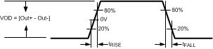 Figure 1. Output Rise And Fall Transition Time
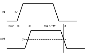 Figure 2. Propagation Delay Timing Diagram
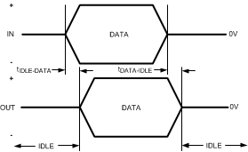 Figure 3. Transmit Idle-Data and Data-Idle Response Time
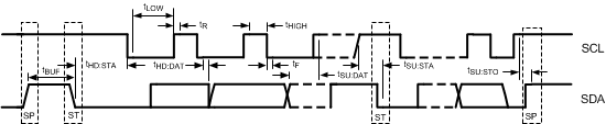 Figure 4. SMBus Timing Parameters
6.8 Typical Characteristics
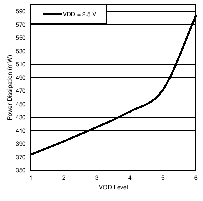
| EQ | Level 4 |
| VOD_DB | 000'b |
| T | 25°C |
| Data Rate, Test Pattern | 1.5625 Gbps, 1010 Pattern |
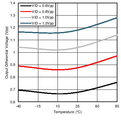
| VOD | Level 6 |
| EQ | Level 1 |
| VDD | 2.5 V |
| Data Rate, Test Pattern | 1.5625 Gbps, 1010 Pattern |
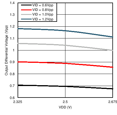
| VOD | Level 6 |
| EQ | Level 1 |
| T | 25°C |
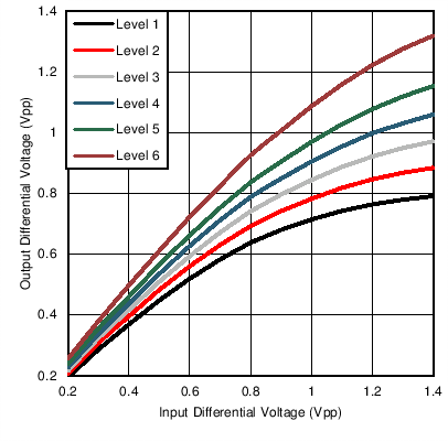
A.
Figure 8. Typical VOD vs. VID
| Data Rate, Test Pattern | 1.5625 Gbps, 1010 Pattern |
| EQ | Level 1 |
| T | 25°C |
| VDD | 2.5 V |