ZHCSER7C October 2015 – November 2018 DRV8885
PRODUCTION DATA.
- 1 特性
- 2 应用
- 3 说明
- 4 修订历史记录
- 5 Pin Configuration and Functions
- 6 Specifications
-
7 Detailed Description
- 7.1 Overview
- 7.2 Functional Block Diagram
- 7.3
Feature Description
- 7.3.1 Stepper Motor Driver Current Ratings
- 7.3.2 PWM Motor Drivers
- 7.3.3 Microstepping Indexer
- 7.3.4 Current Regulation
- 7.3.5 Controlling RREF With an MCU
- 7.3.6 Decay Modes
- 7.3.7 Blanking Time
- 7.3.8 Charge Pump
- 7.3.9 LDO Voltage Regulator
- 7.3.10 Logic and Multi-Level Pin Diagrams
- 7.3.11 Protection Circuits
- 7.4 Device Functional Modes
- 8 Application and Implementation
- 9 Power Supply Recommendations
- 10Layout
- 11器件和文档支持
- 12机械、封装和可订购信息
封装选项
机械数据 (封装 | 引脚)
散热焊盘机械数据 (封装 | 引脚)
订购信息
7.3.4 Current Regulation
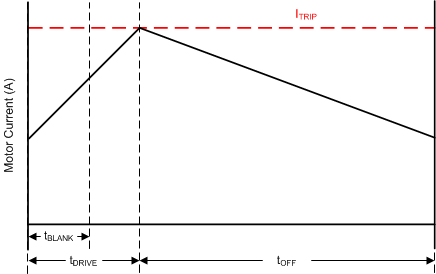
The current through the motor windings is regulated by an adjustable fixed-off-time PWM current regulation circuit. When an H-bridge is enabled, current rises through the winding at a rate dependent on the DC voltage, inductance of the winding, and the magnitude of the back EMF present. Once the current hits the current chopping threshold, the bridge enters a decay mode for a fixed, 20 μs, period of time to decrease the current. After the off time expires, the bridge is re-enabled, starting another PWM cycle.
 Figure 14. Current Chopping Waveform
 The PWM chopping current is set by a comparator which looks at the voltage across current sense FETs in parallel with the low-side drivers. The current sense FETs are biased with a reference current that is the output of a current-mode sine-weighted DAC whose full-scale reference current is set by the current through the RREF pin. An external resistor is placed from the RREF pin to GND in order to set the reference current. In addition, the TRQ pin can further scale the reference current.
The chopping current is calculated as follows:

Example: If a 30-kΩ resistor is connected to the RREF pin, the chopping current will be 1 A (TRQ at 100%)
The TRQ pin is the input to a DAC used to scale the output current. The current scalar value for different inputs is shown below.
Table 5. Torque DAC Settings
| TRQ | CURRENT SCALAR (TRQ) |
|---|---|
| 0 | 100% |
| Z | 75% |
| 1 | 50% |