SLVSF66A August   2019  – December  2019 DRV8874

PRODUCTION DATA.  

  1. Features
  2. Applications
  3. Description
    1.     Device Images
      1.      Simplified Schematic
  4. Revision History
  5. Pin Configuration and Functions
    1.     Pin Functions
  6. Specifications
    1. 6.1 Absolute Maximum Ratings
    2. 6.2 ESD Ratings
    3. 6.3 Recommended Operating Conditions
    4. 6.4 Thermal Information
    5. 6.5 Electrical Characteristics
    6. 6.6 Typical Characteristics
  7. Detailed Description
    1. 7.1 Overview
    2. 7.2 Functional Block Diagram
    3. 7.3 Feature Description
      1. 7.3.1 External Components
      2. 7.3.2 Control Modes
        1. 7.3.2.1 PH/EN Control Mode (PMODE = Logic Low)
        2. 7.3.2.2 PWM Control Mode (PMODE = Logic High)
        3. 7.3.2.3 Independent Half-Bridge Control Mode (PMODE = Hi-Z)
      3. 7.3.3 Current Sense and Regulation
        1. 7.3.3.1 Current Sensing
        2. 7.3.3.2 Current Regulation
          1. 7.3.3.2.1 Fixed Off-Time Current Chopping
          2. 7.3.3.2.2 Cycle-By-Cycle Current Chopping
      4. 7.3.4 Protection Circuits
        1. 7.3.4.1 VM Supply Undervoltage Lockout (UVLO)
        2. 7.3.4.2 VCP Charge Pump Undervoltage Lockout (CPUV)
        3. 7.3.4.3 OUTx Overcurrent Protection (OCP)
        4. 7.3.4.4 Thermal Shutdown (TSD)
        5. 7.3.4.5 Fault Condition Summary
      5. 7.3.5 Pin Diagrams
        1. 7.3.5.1 Logic-Level Inputs
        2. 7.3.5.2 Tri-Level Inputs
        3. 7.3.5.3 Quad-Level Inputs
    4. 7.4 Device Functional Modes
      1. 7.4.1 Active Mode
      2. 7.4.2 Low-Power Sleep Mode
      3. 7.4.3 Fault Mode
  8. Application and Implementation
    1. 8.1 Application Information
    2. 8.2 Typical Application
      1. 8.2.1 Primary Application
        1. 8.2.1.1 Design Requirements
        2. 8.2.1.2 Detailed Design Procedure
          1. 8.2.1.2.1 Current Sense and Regulation
          2. 8.2.1.2.2 Power Dissipation and Output Current Capability
          3. 8.2.1.2.3 Thermal Performance
            1. 8.2.1.2.3.1 Steady-State Thermal Performance
            2. 8.2.1.2.3.2 Transient Thermal Performance
        3. 8.2.1.3 Application Curves
      2. 8.2.2 Alternative Application
        1. 8.2.2.1 Design Requirements
        2. 8.2.2.2 Detailed Design Procedure
          1. 8.2.2.2.1 Current Sense and Regulation
        3. 8.2.2.3 Application Curves
  9. Power Supply Recommendations
    1. 9.1 Bulk Capacitance
  10. 10Layout
    1. 10.1 Layout Guidelines
    2. 10.2 Layout Example
      1. 10.2.1 HTSSOP Layout Example
  11. 11Device and Documentation Support
    1. 11.1 Documentation Support
      1. 11.1.1 Related Documentation
    2. 11.2 Receiving Notification of Documentation Updates
    3. 11.3 Community Resources
    4. 11.4 Trademarks
    5. 11.5 Electrostatic Discharge Caution
    6. 11.6 Glossary
  12. 12Mechanical, Packaging, and Orderable Information

封装选项

机械数据 (封装 | 引脚)
散热焊盘机械数据 (封装 | 引脚)
订购信息

Pin Configuration and Functions

DRV8874 PWP Package
16-Pin HTSSOP With Exposed Thermal Pad
Top View
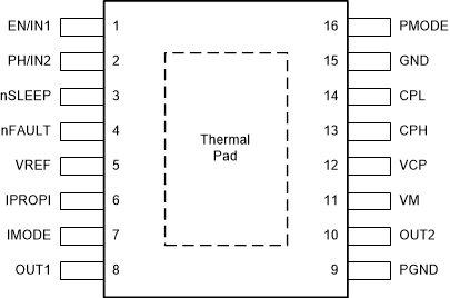
DRV8874 drv887x-pinout-tssop.gif

Pin Functions

PIN TYPE DESCRIPTION
NAME PWP
CPH 13 PWR Charge pump switching node. Connect a X5R or X7R, 22-nF, VM-rated ceramic capacitor between the CPH and CPL pins.
CPL 14 PWR
EN/IN1 1 I H-bridge control input. See Control Modes. Internal pulldown resistor.
GND 15 PWR Device ground. Connect to system ground.
IMODE 7 I Current regulation and overcurrent protection mode. See Current Regulation. Quad-level input.
IPROPI 6 O Analog current output proportional to load current. See Current Sensing.
nFAULT 4 OD Fault indicator output. Pulled low during a fault condition. Connect an external pullup resistor for open-drain operation. See Protection Circuits.
nSLEEP 3 I Sleep mode input. Logic high to enable device. Logic low to enter low-power sleep mode. See Device Functional Modes. Internal pulldown resistor.
OUT1 8 O H-bridge output. Connect to the motor or other load.
OUT2 10 O H-bridge output. Connect to the motor or other load.
PGND 9 PWR Device power ground. Connect to system ground.
PH/IN2 2 I H-bridge control input. See Control Modes. Internal pulldown resistor.
PMODE 16 I H-bridge control input mode. See Control Modes. Tri-level input.
VCP 12 PWR Charge pump output. Connect a X5R or X7R, 100-nF, 16-V ceramic capacitor between the VCP and VM pins.
VM 11 PWR 4.5-V to 37-V power supply input. Connect a 0.1-µF bypass capacitor to ground, as well as sufficient Bulk Capacitance rated for VM.
VREF 5 I External reference voltage input to set internal current regulation limit. See Current Regulation.
PAD Thermal pad. Connect to system ground.