SLVSF66A August   2019  – December  2019 DRV8874

PRODUCTION DATA.  

  1. Features
  2. Applications
  3. Description
    1.     Device Images
      1.      Simplified Schematic
  4. Revision History
  5. Pin Configuration and Functions
    1.     Pin Functions
  6. Specifications
    1. 6.1 Absolute Maximum Ratings
    2. 6.2 ESD Ratings
    3. 6.3 Recommended Operating Conditions
    4. 6.4 Thermal Information
    5. 6.5 Electrical Characteristics
    6. 6.6 Typical Characteristics
  7. Detailed Description
    1. 7.1 Overview
    2. 7.2 Functional Block Diagram
    3. 7.3 Feature Description
      1. 7.3.1 External Components
      2. 7.3.2 Control Modes
        1. 7.3.2.1 PH/EN Control Mode (PMODE = Logic Low)
        2. 7.3.2.2 PWM Control Mode (PMODE = Logic High)
        3. 7.3.2.3 Independent Half-Bridge Control Mode (PMODE = Hi-Z)
      3. 7.3.3 Current Sense and Regulation
        1. 7.3.3.1 Current Sensing
        2. 7.3.3.2 Current Regulation
          1. 7.3.3.2.1 Fixed Off-Time Current Chopping
          2. 7.3.3.2.2 Cycle-By-Cycle Current Chopping
      4. 7.3.4 Protection Circuits
        1. 7.3.4.1 VM Supply Undervoltage Lockout (UVLO)
        2. 7.3.4.2 VCP Charge Pump Undervoltage Lockout (CPUV)
        3. 7.3.4.3 OUTx Overcurrent Protection (OCP)
        4. 7.3.4.4 Thermal Shutdown (TSD)
        5. 7.3.4.5 Fault Condition Summary
      5. 7.3.5 Pin Diagrams
        1. 7.3.5.1 Logic-Level Inputs
        2. 7.3.5.2 Tri-Level Inputs
        3. 7.3.5.3 Quad-Level Inputs
    4. 7.4 Device Functional Modes
      1. 7.4.1 Active Mode
      2. 7.4.2 Low-Power Sleep Mode
      3. 7.4.3 Fault Mode
  8. Application and Implementation
    1. 8.1 Application Information
    2. 8.2 Typical Application
      1. 8.2.1 Primary Application
        1. 8.2.1.1 Design Requirements
        2. 8.2.1.2 Detailed Design Procedure
          1. 8.2.1.2.1 Current Sense and Regulation
          2. 8.2.1.2.2 Power Dissipation and Output Current Capability
          3. 8.2.1.2.3 Thermal Performance
            1. 8.2.1.2.3.1 Steady-State Thermal Performance
            2. 8.2.1.2.3.2 Transient Thermal Performance
        3. 8.2.1.3 Application Curves
      2. 8.2.2 Alternative Application
        1. 8.2.2.1 Design Requirements
        2. 8.2.2.2 Detailed Design Procedure
          1. 8.2.2.2.1 Current Sense and Regulation
        3. 8.2.2.3 Application Curves
  9. Power Supply Recommendations
    1. 9.1 Bulk Capacitance
  10. 10Layout
    1. 10.1 Layout Guidelines
    2. 10.2 Layout Example
      1. 10.2.1 HTSSOP Layout Example
  11. 11Device and Documentation Support
    1. 11.1 Documentation Support
      1. 11.1.1 Related Documentation
    2. 11.2 Receiving Notification of Documentation Updates
    3. 11.3 Community Resources
    4. 11.4 Trademarks
    5. 11.5 Electrostatic Discharge Caution
    6. 11.6 Glossary
  12. 12Mechanical, Packaging, and Orderable Information

封装选项

机械数据 (封装 | 引脚)
散热焊盘机械数据 (封装 | 引脚)
订购信息

Control Modes

The DRV887x family of devices provides three modes to support different control schemes with the EN/IN1 and PH/IN2 pins. The control mode is selected through the PMODE pin with either logic low, logic high, or setting the pin Hi-Z as shown in Table 2. The PMODE pin state is latched when the device is enabled through the nSLEEP pin. The PMODE state can be changed by taking the nSLEEP pin logic low, waiting the tSLEEP time, changing the PMODE pin input, and then enabling the device by taking the nSLEEP pin back logic high.

Table 2. PMODE Functions

PMODE STATE CONTROL MODE
PMODE = Logic Low PH/EN
PMODE = Logic High PWM
PMODE = Hi-Z Independent Half-Bridge
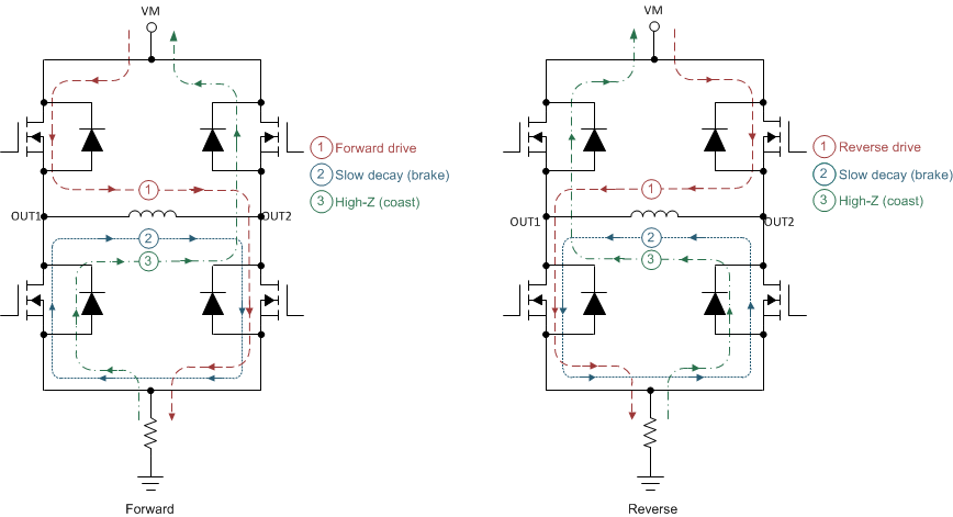
DRV8874 bridge_control_slvsds7.gifFigure 10. H-Bridge States

The inputs can accept static or pulse-width modulated (PWM) voltage signals for either 100% or PWM drive modes. The device input pins can be powered before VM is applied with no issues. By default, the EN/IN1 and PH/IN2 pins have an internal pulldown resistor to ensure the outputs are Hi-Z if no inputs are present.

The sections below show the truth table for each control mode. Note that these tables do not take into account the internal current regulation feature. Additionally, the DRV887x family of devices automatically handles the dead-time generation when switching between the high-side and low-side MOSFET of a half-bridge.

Figure 10 describes the naming and configuration for the various H-bridge states.