ZHCSFQ0 November 2016 DRV8872-Q1
PRODUCTION DATA.
8 Application and Implementation
NOTE
Information in the following applications sections is not part of the TI component specification, and TI does not warrant its accuracy or completeness. TI’s customers are responsible for determining suitability of components for their purposes. Customers should validate and test their design implementation to confirm system functionality.
8.1 Application Information
The DRV8872-Q1 device is typically used to drive one brushed DC motor.
8.2 Typical Application
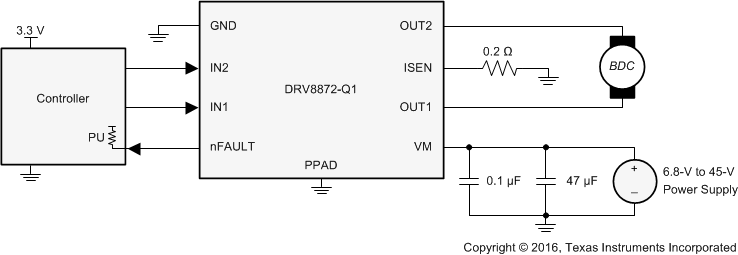 Figure 7. Typical Connections
8.2.1 Design Requirements
Table 3 lists the design parameters.
Table 3. Design Parameters
| DESIGN PARAMETER | REFERENCE | EXAMPLE VALUE |
|---|---|---|
| Motor voltage | VM | 24 V |
| Motor RMS current | IRMS | 0.8 A |
| Motor startup current | ISTART | 2 A |
| Motor current trip point | ITRIP | 2.2 A |
| Sense resistance | RISEN | 0.16 Ω |
| PWM frequency | fPWM | 5 kHz |
8.2.2 Detailed Design Procedure
8.2.2.1 Motor Voltage
The motor voltage used depends on the ratings of the motor selected and the desired RPM. A higher voltage spins a brushed DC motor faster with the same PWM duty cycle applied to the power FETs. A higher voltage also increases the rate of current change through the inductive motor windings.
8.2.2.2 Drive Current
The current path is through the high-side sourcing DMOS power driver, motor winding, and low-side sinking DMOS power driver. Power dissipation losses in one source and sink DMOS power driver are shown in Equation 2.

The DRV8872-Q1 device has been measured to be capable of 2-A RMS current at 25°C on standard FR-4 PCBs. The maximum RMS current varies based on the PCB design, ambient temperature, and PWM frequency. Typically, switching the inputs at 200 kHz compared to 20 kHz causes 20% more power loss in heat.
8.2.2.3 Sense Resistor
For optimal performance, the sense resistor must have the features that follow:
- Surface-mount device
- Low inductance
- Rated for high enough power
- Placed closely to the motor driver
The power dissipated by the sense resistor equals IRMS 2 × R. For example, if peak motor current is 3 A, RMS motor current is 1.5 A, and a 0.2-Ω sense resistor is used, the resistor dissipates 1.5 A2 × 0.2 Ω = 0.45 W. The power quickly increases with higher current levels.
Resistors typically have a rated power within some ambient temperature range, along with a derated power curve for high ambient temperatures. When a PCB is shared with other components generating heat, the system designer should add margin. It is always best to measure the actual sense resistor temperature in a final system.
Because power resistors are larger and more expensive than standard resistors, multiple standard resistors can be used in parallel, between the sense node and ground. This configuration distributes the current and heat dissipation.
8.2.3 Application Curves
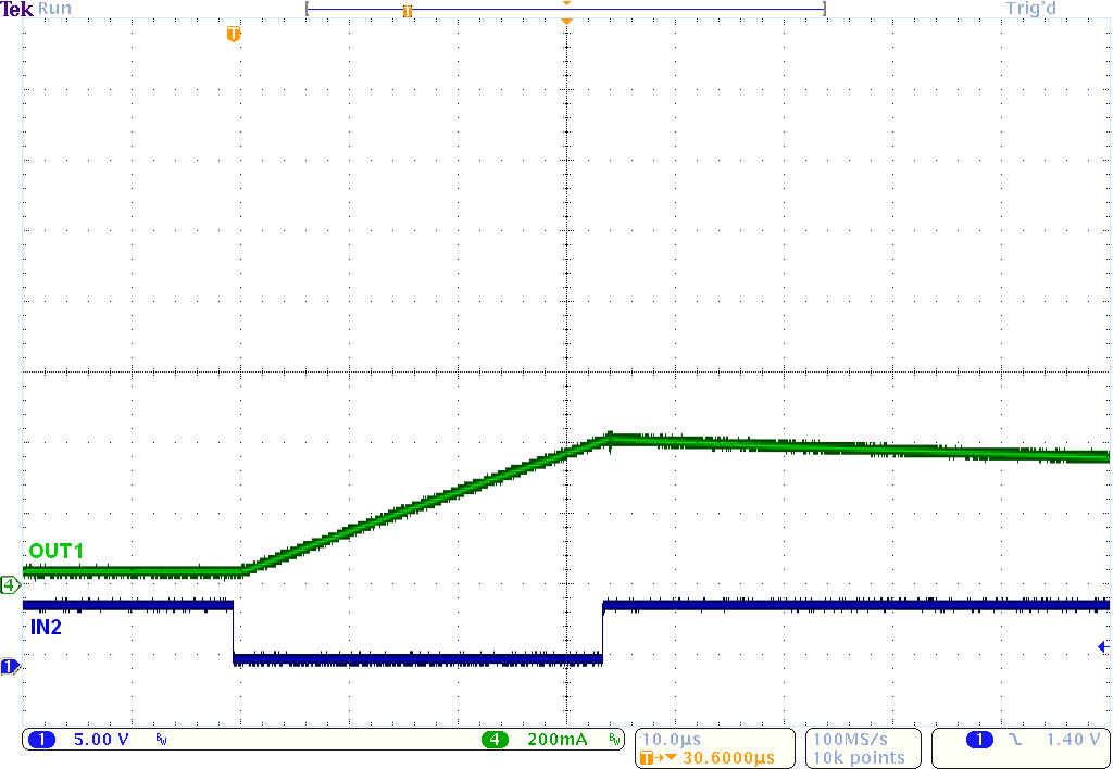 Figure 8. Current Ramp With a 2-Ω, 1 mH,
 RL Load and VM = 12 V
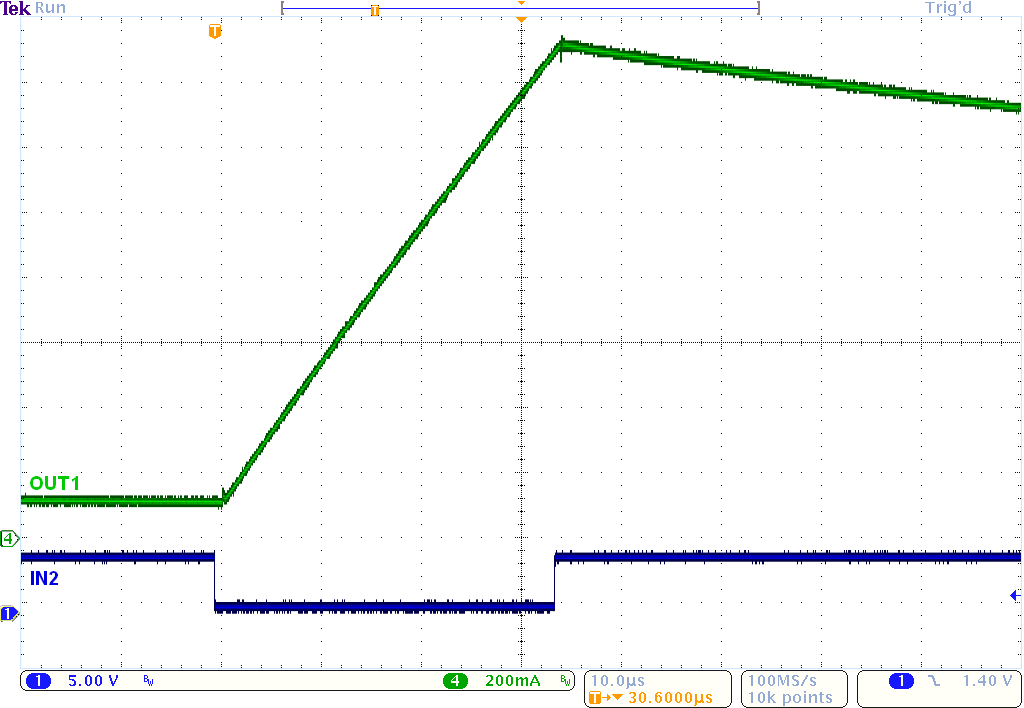 Figure 10. Current Ramp With a 2-Ω, 1 mH,
 RL Load and VM = 45 V
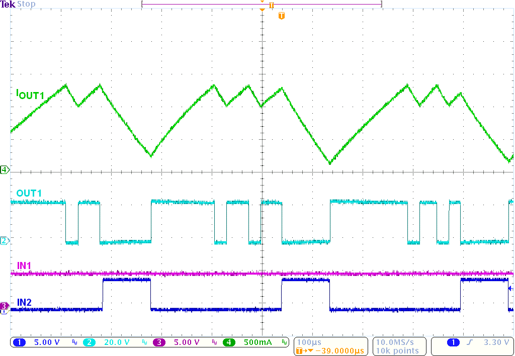 Figure 12. Current Regulation With RSENSE = 0.26 Ω
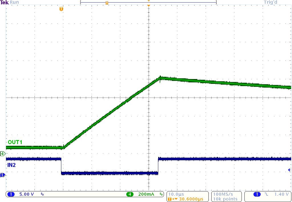 Figure 9. Current Ramp With a 2-Ω, 1 mH,
 RL Load and VM = 24 V
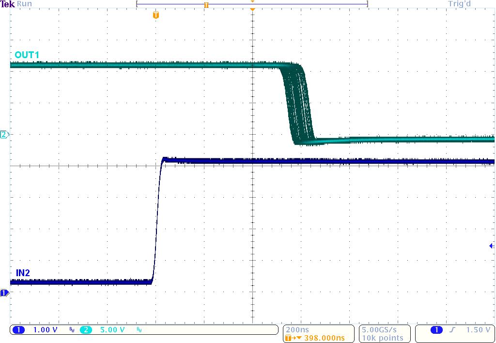 Figure 11. tPD
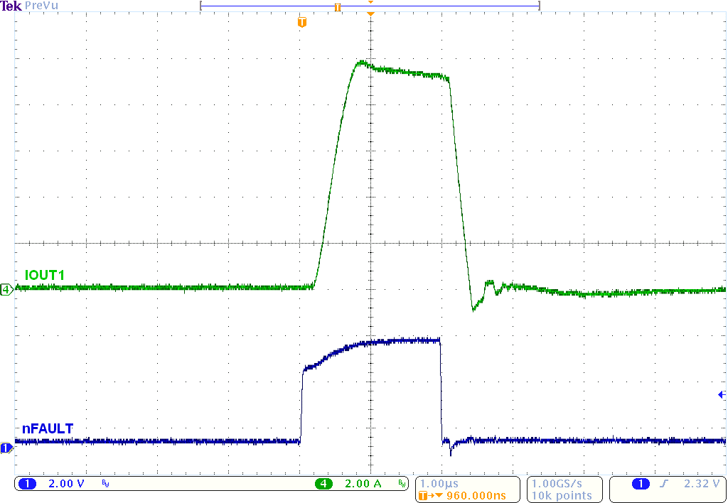 Figure 13. OCP With 24 V and Outputs Shorted Together