SLVSAW3D July 2011 – January 2016 DRV8805
PRODUCTION DATA.
- 1 Features
- 2 Applications
- 3 Description
- 4 Revision History
- 5 Pin Configuration and Functions
- 6 Specifications
- 7 Detailed Description
- 8 Application and Implementation
- 9 Power Supply Recommendations
- 10Layout
- 11Device and Documentation Support
- 12Mechanical, Packaging, and Orderable Information
封装选项
机械数据 (封装 | 引脚)
散热焊盘机械数据 (封装 | 引脚)
- PWP|16
订购信息
8 Application and Implementation
NOTE
Information in the following applications sections is not part of the TI component specification, and TI does not warrant its accuracy or completeness. TI’s customers are responsible for determining suitability of components for their purposes. Customers should validate and test their design implementation to confirm system functionality.
8.1 Application Information
The DRV8805 can be used to drive one unipolar stepper motor.
8.2 Typical Application
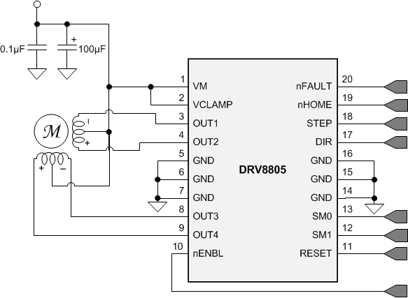 Figure 7. Typical Application Schematic
8.2.1 Design Requirements
Table 5 lists the design parameters for this design example.
Table 5. Design Parameters
| DESIGN PARAMETER | REFERENCE | EXAMPLE VALUE |
|---|---|---|
| Supply Voltage | VM | 24 V |
| Motor Winding Resistance | RL | 7.4 Ω/phase |
| Motor Full Step Angle | θstep | 1.8°/step |
| Motor Rated Current | IRATED | 0.75 A |
| PWM frequency | fPWM | 31.25 kHz |
8.2.2 Detailed Design Procedure
8.2.2.1 Motor Voltage
The motor voltage to use will depend on the ratings of the motor selected and the desired torque. A higher voltage shortens the current rise time in the coils of the stepper motor allowing the motor to produce a greater average torque. Using a higher voltage also allows the motor to operate at a faster speed than a lower voltage.
8.2.2.2 Drive Current
The current path is starts from the supply VM, moves through the inductive winding load, and low-side sinking NMOS power FET. Power dissipation losses in one sink NMOS power FET are shown in the following equation.
The DRV8805 has been measured to be capable of 1.5-A Single Channel or 800-mA Four Channels with the DW package and 2-A Single Channel or 1-A Four Channels with the PWP package at 25°C on standard FR-4 PCBs. The maximum RMS current will vary based on PCB design and the ambient temperature.
8.2.3 Application Curves
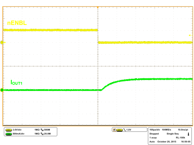
RL Load and VM = 8.2 V
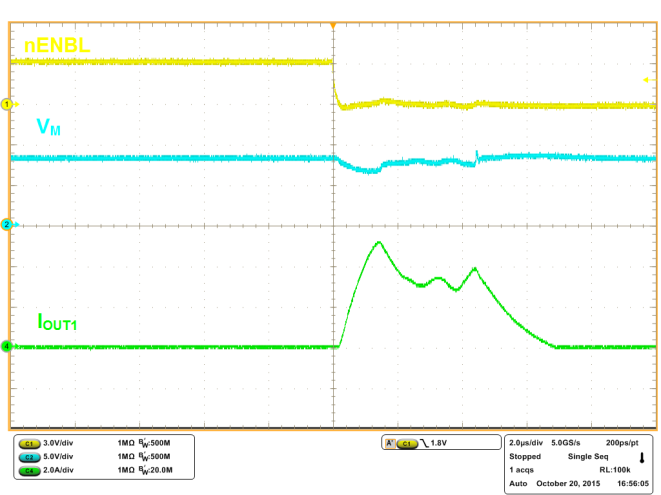
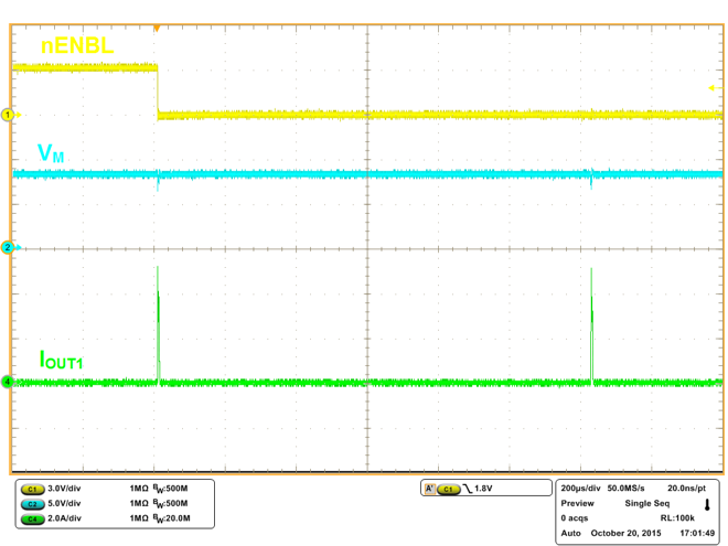
OUT1 Shorted to VM
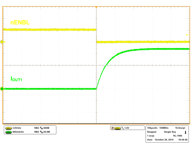
1-mH RL Load and VM = 30 V
