ZHCS218F July 2011 – December 2015 DRV8804
PRODUCTION DATA.
- 1 特性
- 2 应用
- 3 说明
- 4 修订历史记录
- 5 Pin Configuration and Functions
- 6 Specifications
- 7 Detailed Description
- 8 Application and Implementation
- 9 Power Supply Recommendations
- 10Layout
- 11器件和文档支持
- 12机械、封装和可订购信息
封装选项
机械数据 (封装 | 引脚)
散热焊盘机械数据 (封装 | 引脚)
- PWP|16
订购信息
7 Detailed Description
7.1 Overview
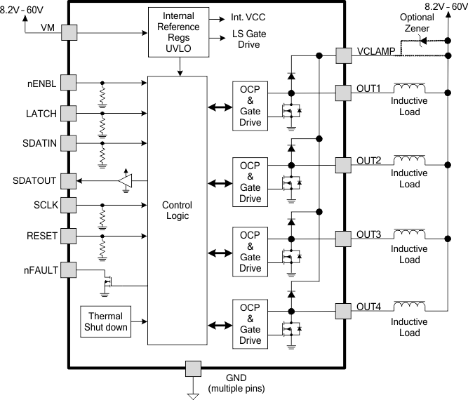
The DRV8804 is an integrated 4-channel low side driver solution for a low side switch application. A serial interface controls the low-side driver outputs and allows for multiple drivers to be chained together and save space on communication lines. The four low-side driver outputs consist of four N-channel MOSFETs that have a typical RDS(on) of 500 mΩ. A single motor supply input VM serves as device power and is internally regulated to power the low side gate drive. The device outputs can be disabled by bringing nENBL pin logic high. This device has several safety features including integrated overcurrent protection that limits the motor current to a fixed maximum above which the device will shut down. Thermal shutdown protection enables the device to automatically shut down if the die temperature exceeds a TTSD limit and will restart once the die reaches a safe temperature. UVLO protection will disable all circuitry in the device if VM drops below the undervoltage lockout threshold.
7.3 Feature Description
7.3.1 Output Drivers
The DRV8804 contains four protected low-side drivers. Each output has an integrated clamp diode connected to a common pin, VCLAMP.
VCLAMP can be connected to the main power supply voltage, VM. It can also be connected to a Zener or TVS diode to VM, allowing the switch voltage to exceed the main supply voltage VM. This connection can be beneficial when driving loads that require very fast current decay, such as unipolar stepper motors.
In all cases, the voltage on the outputs must not be allowed to exceed the maximum output voltage specification.
7.3.2 Serial Interface Operation
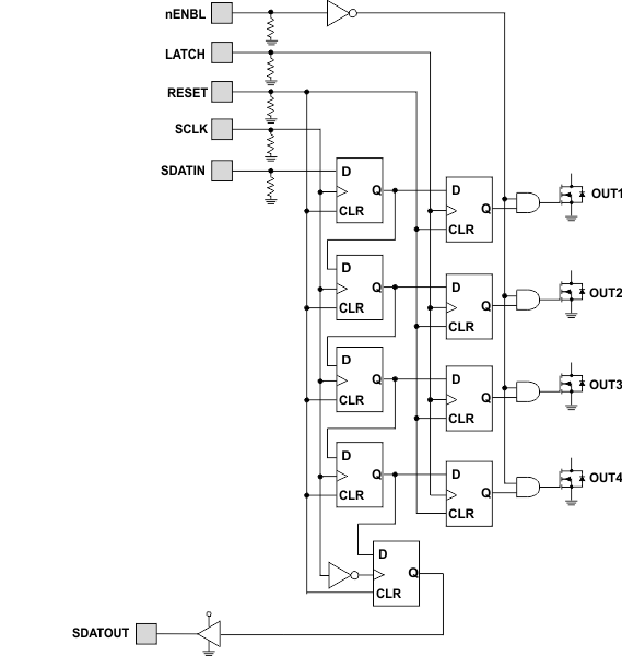
The DRV8804 is controlled with a simple serial interface. Logically, the interface is shown in Figure 6.
Data is shifted into a temporary holding shift register in the part using the SDATIN pin, one bit at each rising edge of the SCLK pin. Data is simultaneously shifted out of the SDATOUT pin, allowing multiple devices to be daisy-chained onto one serial port. Note that the SDATOUT pin has a push-pull driver, which can support driving another DRV8804 SDATIN pin at clock frequencies of up to 1 MHz without an external pullup. A pullup resistor can be used between SDATOUT and an external 5-V logic supply to support higher clock frequencies. TI recommends a resistor value greater than 1 kΩ. The SDATOUT pin is capable of approximately 1-mA source and 5-mA sink. To supply logic signals to a lower-voltage microcontroller, use a resistor divider from SDATOUT to GND.
A rising edge on the LATCH pin latches the data from the temporary shift register into the output stage.
7.3.3 nENBL and RESET Operation
The nENBL pin enables or disables the output drivers. nENBL must be low to enable the outputs. nENBL does not affect the operation of the serial interface logic. Note that nENBL has an internal pulldown.
The RESET pin, when driven active high, resets internal logic, including the OCP fault. All serial interface registers are cleared. Note that RESET has an internal pulldown. An internal power-up reset is also provided, so driving RESET at power up is not required.
7.3.4 Protection Circuits
The DRV8804 is fully protected against undervoltage, overcurrent, and overtemperature events.
7.3.4.1 Overcurrent Protection (OCP)
An analog current limit circuit on each FET limits the current through the FET by removing the gate drive. If this analog current limit persists for longer than the tOCP deglitch time (approximately 3.5 µs), the driver will be disabled and the nFAULT pin will be driven low. The driver will remain disabled for the tRETRY retry time (approximately 1.2 ms), then the fault will be automatically cleared. The fault will be cleared immediately if either RESET pin is activated or VM is removed and re-applied.
7.3.4.2 Thermal Shutdown (TSD)
If the die temperature exceeds safe limits, all output FETs will be disabled and the nFAULT pin will be driven low. Once the die temperature has fallen to a safe level, operation will automatically resume.
7.3.4.3 Undervoltage Lockout (UVLO)
If at any time the voltage on the VM pin falls below the undervoltage lockout (UVLO) threshold voltage, all circuitry in the device will be disabled, and internal logic will be reset. Operation will resume when VM rises above the UVLO threshold.
7.4 Device Functional Modes
When the nENBL pin of the DRV8804 is pulled logic low, the open-drain FET outputs are enabled. Having the device be enabled at logic low allows for the use of long data lines in a high noise environment that do not unintentionally enable the device with coupled noise. The device will still shift data through the SDATIN / SDATOUT lines and SCLK line regardless of the state of the nENBL pin.
Once data has been moved into each of the four shift register lines the LATCH pin can be pulled high to output the state of the four shift registers. Once LATCH is pulled high the state of the four shift registers is placed in a logical AND with the inverse state of the nENBL pin. If the nENBL pin is logic low input and the LATCH pin is logic high the open-drain output of that driver channel will be turned on.
If the device detects that VM has dropped below the UVLO threshold, it will immediately enter a state where all the internal logic is disabled. The device stays in a disabled state until VM rises above the UVLO threshold and all internal logic is then reset. During an Overcurrent Protection (OCP) event the device removes gate drive for one tRETRY interval and the nFAULT pin is driven low. The fault is cleared immediately if RESET is activated or VM is removed and re-applied.

