ZHCS218F July 2011 – December 2015 DRV8804
PRODUCTION DATA.
- 1 特性
- 2 应用
- 3 说明
- 4 修订历史记录
- 5 Pin Configuration and Functions
- 6 Specifications
- 7 Detailed Description
- 8 Application and Implementation
- 9 Power Supply Recommendations
- 10Layout
- 11器件和文档支持
- 12机械、封装和可订购信息
封装选项
机械数据 (封装 | 引脚)
散热焊盘机械数据 (封装 | 引脚)
- PWP|16
订购信息
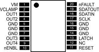
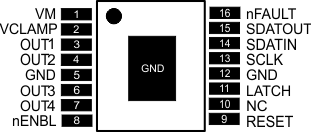
5 Pin Configuration and Functions
DW (Wide SOIC) Package
20-Pin Package
Top View

PWP (HTSSOP)
16-Pin Package
Top View

Pin Functions
| PIN | I/O(1) | DESCRIPTION | EXTERNAL COMPONENTS OR CONNECTIONS |
||
|---|---|---|---|---|---|
| NAME | SOIC | HTSSOP | |||
| POWER AND GROUND | |||||
| GND | 5, 6, 7, 14, 15, 16 |
5, 12, PPAD | — | Device ground | All pins must be connected to GND. |
| VM | 1 | 1 | — | Device power supply | Connect to motor supply (8.2 V - 60 V). |
| CONTROL | |||||
| LATCH | 13 | 11 | I | Latch input | Rising edge latches shift register to output stage – internal pulldown |
| nENBL | 10 | 8 | I | Enable input | Active low enables outputs – internal pulldown |
| RESET | 11 | 9 | I | Reset input | Active-high reset input initializes internal logic – internal pulldown |
| SCLK | 17 | 13 | I | Serial clock | Serial clock input – internal pulldown |
| SDATIN | 18 | 14 | I | Serial data input | Serial data input – internal pulldown |
| SDATOUT | 19 | 15 | O | Serial data output | Serial data output; push-pull structure; see serial interface section for details |
| STATUS | |||||
| nFAULT | 20 | 16 | OD | Fault | Logic low when in fault condition (overtemperature, overcurrent) |
| OUTPUT | |||||
| OUT1 | 3 | 3 | O | Output 1 | Connect to load 1 |
| OUT2 | 4 | 4 | O | Output 2 | Connect to load 2 |
| OUT3 | 8 | 6 | O | Output 3 | Connect to load 3 |
| OUT4 | 9 | 7 | O | Output 4 | Connect to load 4 |
| VCLAMP | 2 | 2 | — | Output clamp voltage | Connect to VM supply, or zener diode to VM supply |
(1) Directions: I = input, O = output, OD = open-drain output