SLOS629D July 2010 – October 2016 DRV8601
PRODUCTION DATA.
- 1 Features
- 2 Applications
- 3 Description
- 4 Revision History
- 5 Pin Configuration and Functions
- 6 Specifications
- 7 Detailed Description
- 8 Application and Implementation
- 9 Power Supply Recommendations
- 10Layout
- 11Device and Documentation Support
- 12Mechanical, Packaging, and Orderable Information
封装选项
机械数据 (封装 | 引脚)
散热焊盘机械数据 (封装 | 引脚)
- DRB|8
订购信息
8 Application and Implementation
NOTE
Information in the following applications sections is not part of the TI component specification, and TI does not warrant its accuracy or completeness. TI’s customers are responsible for determining suitability of components for their purposes. Customers should validate and test their design implementation to confirm system functionality.
8.1 Application Information
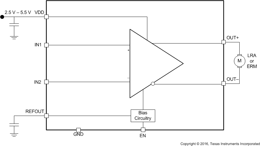
The DRV8601 is intended to be used for haptic applications in a portable product that already has an application processor with analog output interface. As DRV8601 accepts PWM input, it can be directly hooked up to the processor GPIO and can drive PWM outputs.
 Figure 15. Typical Application Block Diagram
DRV8601 can be operated in different instances as listed in Typical Applications which facilitates in the design process for system engineers.
8.2 Typical Applications
8.2.1 Pseudo-Differential Feedback with Internal Reference
8.2.1.1 Design Requirements
The parameters are located in Table 2.
Table 2. Design Parameters
| PARAMETER | EXAMPLE |
|---|---|
| Power supply | 2.5 V – 5.5 V |
| Host processor | PWM output |
| GPIO control | |
| Actuator type | LRA or ERMs |
8.2.1.2 Detailed Design Procedure
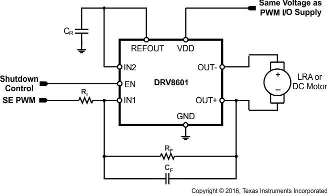
In the pseudo-differential feedback configuration (Figure 16), feedback is taken from only one of the output pins, thereby reducing the number of external components required for the solution. The DRV8601 has an internal reference voltage generator which keeps the REFOUT voltage at VDD/2. The internal reference voltage can be used if and only if the PWM voltage is the same as the supply voltage of the DRV8601 (if VPWM = VDD, as assumed in this section).
Having VPWM= VDD ensures that there is no voltage signal applied to the motor at a PWM duty cycle of 50%. This is a convenient way of temporarily stopping the motor without powering off the DRV8601. Also, this configuration ensures that the direction of rotation of the motor changes when crossing a PWM duty cycle of 50% in both directions. For example, if an ERM motor rotates in the clockwise direction at 20% duty cycle, it will rotate in the counter-clockwise direction at 80% duty cycle at nearly the same speed.
Mathematically, the output voltage is given by Equation 1:

where
- sRFCF is the Laplace Transform variable
- VIN is the single-ended input voltage
RF is normally set equal to RI (RF = RI) so that an overdrive voltage of VDD is achieved when the PWM duty cycle is set to 100%. The optional feedback capacitor, CF, forms a low-pass filter together with the feedback resistor RF, and therefore, the output differential voltage is a function of the average value of the input PWM signal. When driving a motor, design the cutoff frequency of the low-pass filter to be sufficiently lower than the PWM frequency in order to eliminate the PWM frequency and its harmonics from entering the motor. This is desirable when driving motors which do not sufficiently reject the PWM frequency by themselves. When driving a linear vibrator in this configuration, if the feedback capacitor CF is used, care must be taken to make sure that the low-pass cutoff frequency is higher than the resonant frequency of the linear vibrator.
When driving motors which can sufficiently reject the PWM frequency by themselves, the feedback capacitor may be eliminated. For this example, the output voltage is given by Equation 2:

where the only difference from Equation 1 is that the filtering action of the capacitor is not present.
Table 3. Component Design Table
| COMPONENT | VALUE |
|---|---|
| CR | 10 nF / 6.3 V |
| RI | 50 K / 0.01% |
| RF | 50 K / 0.01% |
| CF | 0.01 μF / 6.3 V |
8.2.1.3 Application Curves
Table 4 lists the application curves for this application and following applications from Typical Characteristics.
Table 4. Table of Graphs
| FIGURE | ||
|---|---|---|
| Output voltage (High) | vs Load current | Figure 1 |
| Output voltage (Low) | vs Load current | Figure 2 |
| Output voltage | vs Input voltage, RL = 10 Ω | Figure 3 |
| Output voltage | vs Input voltage, RL = 20 Ω | Figure 4 |
| Supply current | vs Supply voltage | Figure 5 |
| Shutdown supply current | vs Supply voltage | Figure 6 |
| Power dissipation | vs Supply voltage | Figure 7 |
| Slew rate | vs Supply voltage | Figure 8 |
| Output transition | vs Time | Figure 9, Figure 10 |
| Startup | vs Time | Figure 11 |
| Shutdown | vs Time | Figure 12 |
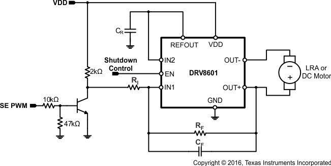
8.2.2 Pseudo-Differential Feedback with Level-Shifter
 Figure 17. Pseudo-Differential Feedback with Level-Shifter
8.2.2.1 Design Requirements
The parameters are located in Table 5.
Table 5. Design Parameters
| PARAMETER | EXAMPLE |
|---|---|
| Power supply | 2.5 V – 5.5 V |
| Host processor | PWM output |
| GPIO control | |
| Actuator type | LRA or ERMs |
8.2.2.2 Detailed Design Procedure
This configuration is desirable when a regulated supply voltage for the DRV8601 (VDD) is availble, but that voltage is different than the PWM input voltage (VPWM). A single NPN transistor can be used as a low-cost level shifting solution. This ensures that VIN = VDD even when VPWM ≠ VDD. A regulated supply for the DRV8601 is still recommended in this scenario. If the supply voltage varies, the PWM level shifter output will follow, and this will, in turn, cause a change in vibration strength. However, if the variance is acceptable, the DRV8601 will still operate properly when connected directly to a battery, for example. A 50% duty cycle will still translate to zero vibration strength across the life cycle of the battery. RF is normally set equal to RI (RF = RI) so that an overdrive voltage of VDD is achieved when the PWM duty cycle is set to 100%.
Table 6. Component Design Table
| COMPONENT | VALUE |
|---|---|
| CR | 10 nF / 6.3 V |
| RI | 50 K / 0.01% |
| RF | 50 K / 0.01% |
| CF | 0.01 μF / 6.3 V |
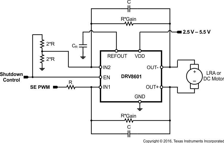
8.2.3 Differential Feedback With External Reference
 Figure 18. Differential Feedback with External Reference
8.2.3.1 Design Requirements
The parameters are located in Table 7.
Table 7. Design Parameters
| PARAMETER | EXAMPLE |
|---|---|
| Power supply | 2.5 V – 5.5 V |
| Host processor | PWM output |
| GPIO control | |
| Gain | 1 |
| Actuator type | LRA or ERMs |
8.2.3.2 Detailed Design Procedure
This configuration is useful for connecting the DRV8601 to an unregulated power supply, most commonly a battery. The gain can then be independently set so that the required motor overdrive voltage can be achieved even when VPWM < VDD. This is often the case when VPWM = 1.8 V, and the desired overdrive voltage is 3.0 V or above. Note that VDD must be greater than or equal to the desired overdrive voltage. A resistor divider can be used to create a VPWM/2 reference for the DRV8601. If the shutdown control voltage is driven by a GPIO in the same supply domain as VPWM, it can be used to supply the resistor divider as in Figure 18 so that no current is drawn by the divider in shutdown.
In this configuration, feedback is taken from both output pins. The output voltage is given by Equation 3:

where
- sRFCF is the Laplace Transform variable
- VIN is the single-ended input voltage
Note that this differs from Equation 1 for the pseudo-differential configuration by a factor of 2 because of differential feedback. The optional feedback capacitor CF forms a low-pass filter together with the feedback resistor RF, and therefore, the output differential voltage is a function of the average value of the input PWM signal VIN. When driving a motor, design the cutoff frequency of the low-pass filter to be sufficiently lower than the PWM frequency in order to eliminate the PWM frequency and its harmonics from entering the motor. This is desirable when driving motors which do not sufficiently reject the PWM frequency by themselves. When driving a linear vibrator in this configuration, if the feedback capacitor CF is used, care must be taken to make sure that the low-pass cutoff frequency is higher than the resonant frequency of the linear vibrator.
When driving motors which can sufficiently reject the PWM frequency by themselves, the feedback capacitor may be eliminated. For this example, the output voltage is given by Equation 4:

Where the only difference from Equation 3 is that the filtering action of the capacitor is not present.
8.2.3.2.1 Selecting Components
8.2.3.2.1.1 Resistors RI and RF
Choose RF and RI in the range of 20 kΩ to 100 kΩ for stable operation.
8.2.3.2.1.2 Capacitor CR
This capacitor filters any noise on the reference voltage generated by the DRV8601 on the REFOUT pin, thereby increasing noise immunity. However, a high value of capacitance results in a large turn-on time. A typical value of 1 nF is recommended for a fast turn-on time. All capacitors should be X5R dielectric or better.
Table 8. Component Design Table
| COMPONENT | VALUE |
|---|---|
| CR | 10 nF / 6.3 V |
| RI | 50 K / 0.01% |
| RF | 50 K / 0.01% |
| CF | 0.01 μF / 6.3 V |
