ZHCSDD3 December 2014 DRV5053-Q1
PRODUCTION DATA.
- 1 特性
- 2 应用
- 3 说明
- 4 输出状态
- 5 修订历史记录
- 6 Pin Configuration and Functions
- 7 Specifications
- 8 Detailed Description
- 9 Application and Implementation
- 10Power Supply Recommendations
- 11器件和文档支持
- 12机械封装和可订购信息
8 Detailed Description
8.1 Overview
The DRV5053-Q1 device is a chopper-stabilized hall sensor with an analog output for magnetic sensing applications. The DRV5053-Q1 device can be powered with a supply voltage between 2.7 and 38 V, and will survive –22 V reverse battery conditions continuously. Note that the DRV5053-Q1 device will not be operating when approximately –22 to 2.4 V is applied to VCC (with respect to GND). In addition, the device can withstand supply voltages up to 40 V for transient durations.
The output voltage is dependent on the magnetic field perpendicular to the package. The absence of a magnetic field will result in OUT = 1 V. A magnetic field will cause the output voltage to change linearly with the magnetic field.
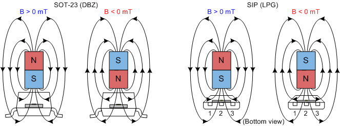
The field polarity is defined as follows: a south pole near the marked side of the package is a positive magnetic field. A north pole near the marked side of the package is a negative magnetic field.
For devices with a negative sensitivity (that is, DRV5053-Q1RA: –40 mV/mT), a south pole will cause the output voltage to drop below 1 V, and a north pole will cause the output to rise above 1 V.
For devices with a positive sensitivity (that is, DRV5053-Q1EA: +40 mV/mT), a south pole will cause the output voltage to rise above 1 V, and a north pole will cause the output to drop below 1 V.
8.2 Functional Block Diagram
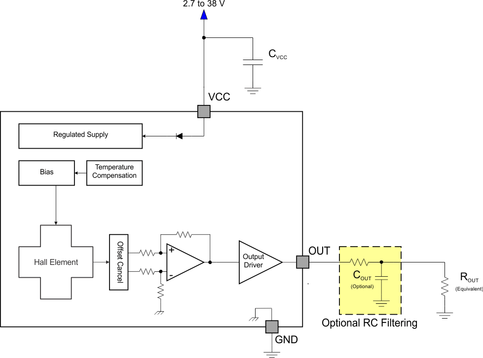
8.3 Feature Description
8.3.1 Field Direction Definition
A positive magnetic field is defined as a south pole near the marked side of the package as shown in Figure 7.
8.3.2 Device Output
The DRV5053-Q1 device output is defined below for negative sensitivity (that is, –45 mV/mT, RA) and positive sensitivity (that is, +45 mV/mT, EA):
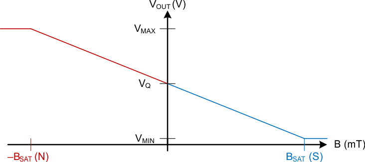 Figure 8. DRV5053-Q1 – Negative Sensitivity
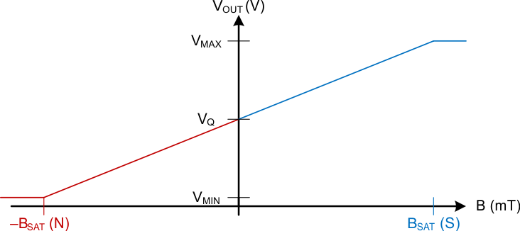 Figure 9. DRV5053-Q1 – Positive Sensitivity
8.3.3 Power-On Time
After applying VCC to the DRV5053-Q1 device, ton must elapse before OUT is valid. Figure 10 shows Case 1 and Figure 11 shows case 2; the output is defined assuming a negative sensitivity device and a constant magnetic field –BSAT < B < BSAT.
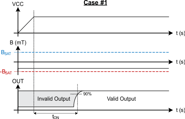 Figure 10. Case 1: Power On When B < 0, North
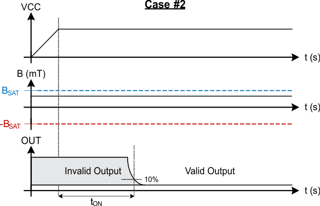 Figure 11. Case 2: Power On When B > 0, South
8.3.4 Output Stage
The DRV5053-Q1 output stage is capable of up to 300 µA of current source or 2.3 mA sink.
For proper operation, ensure that equivalent output load ROUT > 10 kΩ. In addition, ensure that the load capacitance COUT < 10 nF.
8.3.5 Protection Circuits
An analog current limit circuit limits the current through the output driver. The driver current will be clamped to IOCP
8.3.5.1 Overcurrent Protection (OCP)
An analog current-limit circuit limits the current through the FET. The driver current is clamped to IOCP. During this clamping, the rDS(on) of the output FET is increased from the nominal value.
8.3.5.2 Load Dump Protection
The DRV5053-Q1 device operates at DC VCC conditions up to 38 V nominally, and can additionally withstand VCC = 40 V. No current-limiting series resistor is required for this protection.
8.3.5.3 Reverse Supply Protection
The DRV5053-Q1 device is protected in the event that the VCC pin and the GND pin are reversed (up to –22 V).
NOTE
In a reverse supply condition, the OUT pin reverse-current must not exceed the ratings specified in the Absolute Maximum Ratings.
Table 1.
| FAULT | CONDITION | DEVICE | DESCRIPTION | RECOVERY |
|---|---|---|---|---|
| FET overload (OCP) | ISINK ≥ IOCP | Operating | Output current is clamped to IOCP | IO < IOCP |
| Load Dump | 38 V < VCC < 40 V | Operating | Device will operate for a transient duration | VCC ≤ 38 V |
| Reverse Supply | –22 V < VCC < 0 V | Disabled | Device will survive this condition | VCC ≥ 2.7 V |
8.4 Device Functional Modes
The DRV5053-Q1 device is active only when VCC is between 2.7 and 38 V.
When a reverse supply condition exists, the device is inactive.