ZHCSH78B December 2017 – January 2020 DRV5011
PRODUCTION DATA.
- 1 特性
- 2 应用
- 3 说明
- 4 修订历史记录
- 5 Pin Configuration and Functions
- 6 Specifications
- 7 Detailed Description
- 8 Application and Implementation
- 9 Power Supply Recommendations
- 10Layout
- 11器件和文档支持
- 12机械、封装和可订购信息
封装选项
机械数据 (封装 | 引脚)
散热焊盘机械数据 (封装 | 引脚)
- DMR|4
订购信息
5 Pin Configuration and Functions
DBZ Package
3-Pin SOT-23
Top View
DMR Package
4-Pin X2SON With Exposed Thermal Pad
Top View
YBH Package
4-Pin DSBGA
Top View
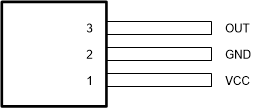
LPG Package
3-Pin TO-92
Top View

Pin Functions
| PIN | I/O | DESCRIPTION | ||||
|---|---|---|---|---|---|---|
| NAME | DSBGA | SOT-23 | X2SON | TO-92 | ||
| GND | A1 | 3 | 2 | 2 | — | Ground reference |
| NC | A2 | — | 3 | — | — | No-connect. This pin is not connected to the silicon. Leave this pin floating or tied to ground, and soldered to the board for mechanical support. |
| OUT | B2 | 2 | 4 | 3 | O | Push-pull CMOS output. Drives a VCC or ground level. |
| VCC | B1 | 1 | 1 | 1 | — | 2.5-V to 5.5-V power supply. TI recommends connecting this pin to a ceramic capacitor to ground with a value of at least 0.01 µF. |
| Thermal Pad | — | — | Thermal Pad | — | — | Leave thermal pad floating or tied to ground, and soldered to the board for mechanical support. |